Welcome to our latest blog post, where we delve into the fascinating world of CMOS VLSI design, focusing on creating the layout of XOR logic gates and 2:1 multiplexers using just six transistors. This exploration is part of the curriculum for the B.Tech. III Year II Semester at the CMOS VLSI DESIGN LABORATORY, JNTUH.
In this post, we will guide you through the step-by-step process of designing and simulating these essential digital components using the Micro Wind tool. This software is widely utilized in educational settings for its efficacy in teaching the nuances of VLSI design through practical implementation.
Our examples aim to illustrate not just the technical steps involved but also the decision-making process in optimizing the design for area, a critical consideration in VLSI design. Whether you’re a student at JNTUH or an enthusiast eager to understand the intricacies of CMOS layouts, this post promises to provide valuable insights into the world of VLSI circuit design. Join us as we explore how these fundamental components are crafted and optimized within the specific framework of the JNTUH curriculum.
Lab Report
AIM: Layout Design and Simulation of XOR and Multiplexer Design
Apparatus / Software required:
- Windows Machine with Microwind Software Installed
Theory:
Understanding NOR and NAND Gates
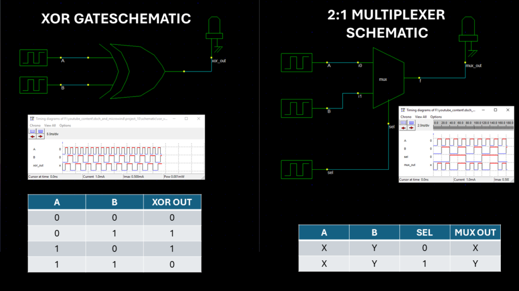
The XOR logic gate and the 2-to-1 multiplexer are fundamental components that play critical roles in various circuits. Both can be efficiently implemented using a compact design involving only six transistors, optimizing space without compromising functionality. This section explores the layout and functionality of these components using the CMOS technology.
XOR Logic Gate
The XOR (Exclusive OR) gate is a digital logic gate that outputs true or high only when the two binary bit inputs to it are unequal. In other words, it outputs a 1 when the number of 1’s inputs is odd, making it essential for arithmetic functions in computers and other digital systems.
The CMOS layout for an XOR gate using six transistors involves two NMOS transistors in series and two PMOS transistors in parallel for each input combination that results in a high output. The gate uses complementary pairs to ensure that when one path turns off, the other turns on, thereby creating the desired XOR functionality.
Table 1: XOR Logic Gate Truth Table
| Input A | Input B | Output (A XOR B) |
|---|---|---|
| 0 | 0 | 0 |
| 0 | 1 | 1 |
| 1 | 0 | 1 |
| 1 | 1 | 0 |
2-to-1 Multiplexer
A 2-to-1 multiplexer is a device that selects one of two available inputs to pass to the output based on a third input, known as the select line. It is widely used in computer systems where resource sharing is needed, such as data routing between multiple sources and a single destination.
The CMOS layout of a 2-to-1 multiplexer using six transistors involves configuring the transistors to act as switches controlled by the select line. Three transistors are connected to each data input, with their gates controlled by the select input to pass either the first or the second data input to the output.
Table 2: 2-to-1 Multiplexer Truth Table
| Select (S) | Input 0 | Input 1 | Output (Based on S) |
|---|---|---|---|
| 0 | X | Y | X |
| 1 | X | Y | Y |
Through these designs, students and professionals alike can learn about the practical applications and efficiency of using CMOS technology to implement crucial digital logic components in compact and effective ways.
The Importance of Schematic to Layout Conversion in CMOS VLSI Design
In CMOS VLSI design, converting a schematic diagram into a physical layout is a critical step. This conversion is essential because it allows designers to visualize and test how an electronic circuit will behave in the real world. By transforming theoretical schematics into tangible layouts, designers can identify potential issues like parasitic capacitance or layout-induced noise, which might not be apparent in the schematic stage. This process also facilitates the integration of multiple transistors onto a single chip, optimizing space and improving performance.
Advantages:
- Accuracy: Converting schematics to layouts helps in achieving precise control over component placement and routing, reducing errors.
- Efficiency: It allows for the efficient use of silicon space, essential in high-density designs like CPUs and memory chips.
- Verification: Physical layouts can be extensively simulated and tested for electrical integrity, ensuring reliability before fabrication.
Disadvantages:
- Complexity: The process can be complex and time-consuming, requiring specialized tools and skills.
- Cost: High-quality design tools and simulations are expensive, increasing the overall cost of development.
- Rigidity: Once a layout is fabricated, making changes can be costly and cumbersome, often requiring significant rework of the design.
Overall, the schematic to layout conversion is a pivotal process in CMOS VLSI design that bridges the gap between theoretical design and practical application, providing a critical check before moving to the production of electronic components.
Procedure:
XOR Gate Layout
- Open the DSCH schematic entry window by clicking on the DSCH icon.
- Select and drag the XOR gate symbol onto the schematic window.
- Drag and drop a clock input into the schematic window.
- Add another clock source in the same manner.
- Drag and drop an LED for the output.
- Connect the inputs and outputs to the XOR gate using the ‘add line’ option.
- Double-click on the components to rename them: rename the output LED to XOR_out, the first clock to clock A, and the second, slower clock to clock B.
- Once setup is complete, click the simulate button, run the simulation, and then stop it to check the XOR gate’s output timing diagram.
- Verify that the output is correct: it should be one when only one of the inputs is one.
- Save the design as xor_v01.sch.
- Go to the file menu, select ‘make Verilog file’ to create the Verilog netlist, then rename and change the extension of the associated text file from .txt to .v.
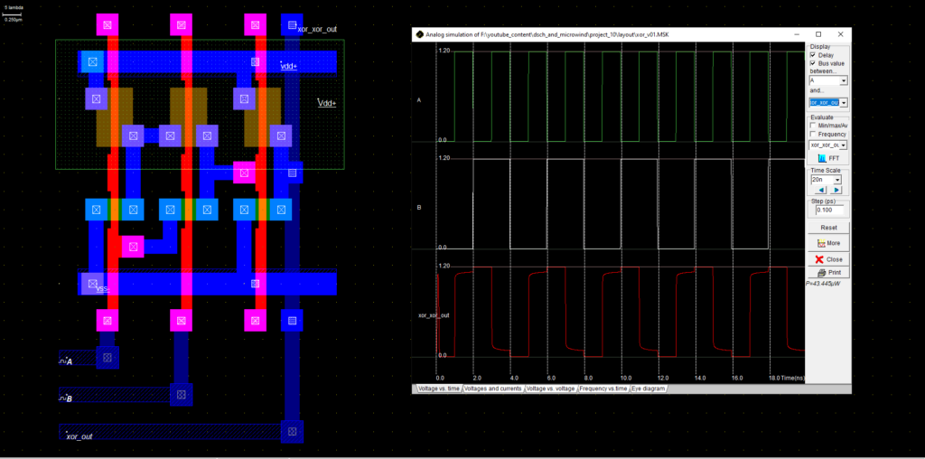
- Open Micro Wind and select the 0.35 micrometer foundry from the file tab.
- Compile the Verilog file by navigating to its location, selecting it, and opening it, then click on ‘compile’.
- Observe that Micro Wind has created an area-optimized six-transistor XOR layout.
- Run the simulation to view the output variations and check the voltage swings.
- Save the layout as xor_v01 layout for future reference.
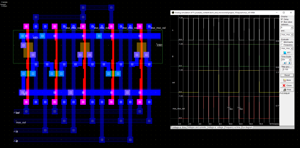
2:1 Multiplexer Design
- Continue with the design of the 2-to-1 multiplexer by starting DSCH and dragging the multiplexer cell design into the schematic window.
- Drag two clock input sources and another clock source for the select line into the schematic, noting that the frequency of B is lower than A.
- Connect the inputs and the select line to the multiplexer and connect the MUX’s output to an LED.
- Run the simulation, then check the timing diagram to verify correct output behavior based on the select line.
- Save the design as mux_v01.sch.
- Create the Verilog netlist from the design, rename the associated text file to .v, and compile it in Micro Wind after selecting the appropriate foundry.
- Run the simulation to verify the multiplexer’s operation and check the power consumption.
- Save the layout as mux_v01.msk for future use.
Results:
After following the steps correctly, the simulation in Microwind show the expected behavior for CMOS XOR gate and 2:1 multiplexer, aligning with the input and output relations defined in the theory section.
Conclusion:
The experiment successfully demonstrates the practical application of schematic to layout conversion for complex designs using DSCH and Microwind.
Viva-Voce Questions:
Here are 20 viva voce questions for a practical based on the CMOS schematic of an XOR gate and a 2:1 multiplexer using the DSCH tool of Microwind, generating a Verilog netlist, converting this Verilog to layout, and then running the simulation, as part of a VLSI CMOS design lab:
XOR Gate
Q1: What is the function of an XOR gate in digital circuits?
- The XOR gate outputs a high level (1) only when the number of high inputs is odd; it is often used for operations like bit addition and parity checking.
Q2: How many transistors are used in the CMOS schematic for an XOR gate as per your lab experiment?
- Six transistors are used to implement the XOR gate in CMOS technology.
Q3: What are the main components of the DSCH tool used in your experiment?
- The main components include the schematic editor for creating designs, the simulation module for testing, and tools for converting schematics into Verilog netlists.
Q4: What does the Verilog netlist represent in the context of XOR gate design?
- The Verilog netlist is a text-based representation of the circuit in Verilog code, describing the connections and functions of the CMOS transistors used in the XOR gate.
Q5: Why is it necessary to convert a Verilog netlist to a layout in VLSI design?
- Converting a Verilog netlist to a layout is necessary for physical realization, allowing designers to visualize and prepare the physical masks needed for fabrication.
Q6: Describe the process of simulating an XOR gate using Microwind.
- Simulation involves loading the generated layout into Microwind, applying input vectors, running the simulation tool, and observing the output to verify correct logic operation.
Q7: What challenges might arise when designing an XOR gate using CMOS technology?
- Challenges include managing power consumption, minimizing area, and ensuring the gate operates correctly under varying electrical conditions.
Q8: How does the layout generated by Microwind for an XOR gate differ from the schematic?
- The layout provides a detailed, spatial representation of the gate including layers, dimensions, and placements of transistors, which differs from the more abstract and symbolic schematic view.
Q9: What are the key outputs to check after simulating an XOR gate in Microwind?
- Key outputs include verifying that the gate logic is correct (i.e., the output matches expected XOR outputs for given inputs) and checking for any layout or design errors.
Q10: How do you ensure that the XOR gate design is optimized for area?
- Area optimization involves carefully arranging transistors to minimize the silicon space required while maintaining functionality and performance.
2:1 Multiplexer
Q11: What is the primary function of a 2:1 multiplexer in digital circuits?
- The primary function of a 2:1 multiplexer is to select one of two inputs to pass to the output based on the state of a third input, known as the select line.
Q12: How many transistors does your 2:1 multiplexer design use?
- Similar to the XOR gate, the 2:1 multiplexer design uses six transistors.
Q13: Explain how you used the DSCH tool for designing the 2:1 multiplexer.
- The DSCH tool was used to create the schematic of the 2:1 multiplexer, placing components and connecting them according to the desired logic function.
Q14: What role does the Verilog netlist play in the design of a 2:1 multiplexer?
- The Verilog netlist describes the logical structure and connections of the 2:1 multiplexer in Verilog language, crucial for subsequent layout generation and simulation.
Q15: Discuss the importance of selecting a proper foundry in Microwind for compiling a Verilog file.
- Selecting a proper foundry in Microwind is crucial because it determines the technology parameters like transistor dimensions and electrical characteristics, directly impacting the performance and scalability of the design.
Q16: Describe the simulation process for a 2:1 multiplexer in Microwind.
- The simulation process involves loading the layout, applying different combinations of inputs and the select line, running the simulation, and observing whether the correct input is passed to the output.
Q17: What challenges are involved in designing a 2:1 multiplexer using CMOS technology?
- Challenges include ensuring the multiplexer switches correctly between inputs with minimal delay and power consumption, and handling the layout complexity to avoid signal integrity issues.
Q18: How can you verify the functionality of a 2:1 multiplexer in a VLSI lab?
- Functionality can be verified by simulating the multiplexer under all possible input states and checking if the output correctly matches the selected input.
Q19: What outputs do you expect when simulating a 2:1 multiplexer, and why are they important?
- Expected outputs are the correct transmission of selected inputs to the output. These are important for validating that the multiplexer operates reliably and as designed.
Q20: What steps are taken to optimize the design of a 2:1 multiplexer in terms of power and area?
- Optimization steps may include minimizing the number of transistors, using efficient gating strategies, and arranging the layout to reduce power consumption and silicon area.
FAQ
Here are 10 FAQ questions based on the practical involving the CMOS schematic of XOR gates and 2:1 multiplexers using the DSCH tool of Microwind:
Q1: What is the purpose of using area-optimized designs in VLSI CMOS circuits?
- Area-optimized designs help in reducing the silicon footprint of the circuits, which can lead to lower costs and potentially lower power consumption.
Q2: Why is it difficult to optimize power, area, and operating frequency simultaneously in VLSI designs?
- These parameters often conflict; for example, decreasing area can increase power density and heat, while increasing operating frequency can increase power consumption and dynamic losses.
Q3: How does the DSCH tool facilitate the design of CMOS circuits like XOR gates and multiplexers?
- DSCH provides a schematic capture environment where designers can visually construct their circuits using CMOS transistors and then automatically generate Verilog netlists for further processing.
Q4: What are the benefits of converting a schematic to a Verilog netlist?
- Converting a schematic to a Verilog netlist allows for digital simulation and synthesis tools to optimize the circuit design before physical layout, ensuring the design meets its specifications.
Q5: How does Microwind assist in the conversion of Verilog to layout?
- Microwind takes the Verilog netlist and converts it into a physical layout, automatically placing and routing the transistors according to predefined rules and the selected technology node.
Q6: What factors are considered when designing an XOR gate in Microwind?
- Key factors include the number of transistors, the configuration of PMOS and NMOS transistors, area optimization, and ensuring the correct logical function and timing characteristics.
Q7: Why does the power consumption of a multiplexer exceed that of an XOR gate, despite both having the same number of transistors?
- The difference in power consumption may arise from the different configurations and switching activities in the circuits, where the multiplexer may experience more frequent or higher energy transitions.
Q8: What is the significance of the pass transistor configuration in XOR and multiplexer circuits?
- Pass transistors control the flow of signals based on other input signals, crucial for functions like signal gating in multiplexers and logical differentiation in XOR gates.
Q9: How do designers prioritize which factor (power, area, frequency) to optimize in a VLSI design using tools like DSCH and Microwind?
- The prioritization depends on the specific requirements of the application; for instance, a wearable device might prioritize low power, while a high-performance computing application might focus on frequency.
Q10: What challenges might arise from the area optimization of XOR and multiplexer circuits in practical VLSI applications?
- Area optimization might lead to increased capacitance and resistance in smaller geometries, potentially affecting signal integrity, speed, and reliability of the circuit.
Internal Links:
- JNTUH VLSI Lab Experiments – Explore a series of lab experiments for understanding VLSI design concepts using Xilinx Vivado.
CMOS VLSI LAB CYCLE 01:
Lab Reports and Related YouTube Videos:
- Lab 01: Logic Gates
- Lab 02: Encoder and Decoder
- Lab 03: Multiplexer, Demultiplexer
- Lab 04: Binary to Gray Converter
- Lab 05: Comparator Circuit
- Lab 06: Adder Circuit
CMOS VLSI LAB CYCLE 02:
Lab Reports and Related YouTube Video:
- Lab 01 Part-2: Basic Logic Gates Layout
- Lab 02 Part-2: Basic Logic Gates Layout
- Lab 02 Part-2: Basic Logic Gates Layout
These resources provide a comprehensive overview and practical insights into various aspects of CMOS VLSI design, offering valuable information for students and enthusiasts interested in exploring the field of VLSI design using Xilinx Vivado and Microwind.