In this detailed exploration, we delve into the practical aspects of designing an 8-to-1 multiplexer and a 1-to-8 demultiplexer, crucial components in the realm of digital and VLSI (Very Large Scale Integration) design. This guide caters to the curriculum of CMOS VLSI Design Laboratory for B.Tech. III Year II Semester, following the JNTUH curriculum for ECE students. From theory to simulation using Xilinx Vivado, this comprehensive blog post aims to enhance your understanding and skills in handling complex digital design processes.
Lab Report
AIM: Design of 8-to-1 multiplexer and 1-to-8 demultiplexer
Apparatus / Software required:
- Xilinx Vivado Design Suite
- Windows Machine
- Notepad or any text editor
Theory:
Multiplexers and demultiplexers are fundamental components in digital circuits, enabling the routing of multiple signals through a single channel. An 8-to-1 multiplexer selects one of the 8 input digital signals and directs it to the single output line, while a 1-to-8 demultiplexer performs the reverse, distributing a single input signal to one of the 8 outputs. The functionality of these devices can be represented as follows:
8-to-1 Multiplexer Detailed Input-Output Relationship
For the 8-to-1 Multiplexer, the output (Y) is directly determined by the select lines (S2, S1, S0). Each row shows how the combination of these select lines chooses one of the eight inputs to be forwarded to the output.
| S2 | S1 | S0 | Output (Y) | Description |
|---|---|---|---|---|
| 0 | 0 | 0 | I0 | Selects input I0 |
| 0 | 0 | 1 | I1 | Selects input I1 |
| 0 | 1 | 0 | I2 | Selects input I2 |
| 0 | 1 | 1 | I3 | Selects input I3 |
| 1 | 0 | 0 | I4 | Selects input I4 |
| 1 | 0 | 1 | I5 | Selects input I5 |
| 1 | 1 | 0 | I6 | Selects input I6 |
| 1 | 1 | 1 | I7 | Selects input I7 |
1-to-8 Demultiplexer Detailed Input-Output Relationship
In the 1-to-8 Demultiplexer, a single input (I) is directed to one of the eight outputs (O0 to O7), based on the combination of the select lines (S2, S1, S0). Each row indicates which output becomes active (carries the input signal) according to the select line values.
| S2 | S1 | S0 | Active Output | Description |
|---|---|---|---|---|
| 0 | 0 | 0 | O0 | Routes I to output O0 |
| 0 | 0 | 1 | O1 | Routes I to output O1 |
| 0 | 1 | 0 | O2 | Routes I to output O2 |
| 0 | 1 | 1 | O3 | Routes I to output O3 |
| 1 | 0 | 0 | O4 | Routes I to output O4 |
| 1 | 0 | 1 | O5 | Routes I to output O5 |
| 1 | 1 | 0 | O6 | Routes I to output O6 |
| 1 | 1 | 1 | O7 | Routes I to output O7 |
These tables clearly illustrate how select lines control the data path in multiplexers and demultiplexers, effectively managing digital signals within a circuit by either consolidating multiple inputs to one output or distributing a single input to multiple outputs.
Procedure:
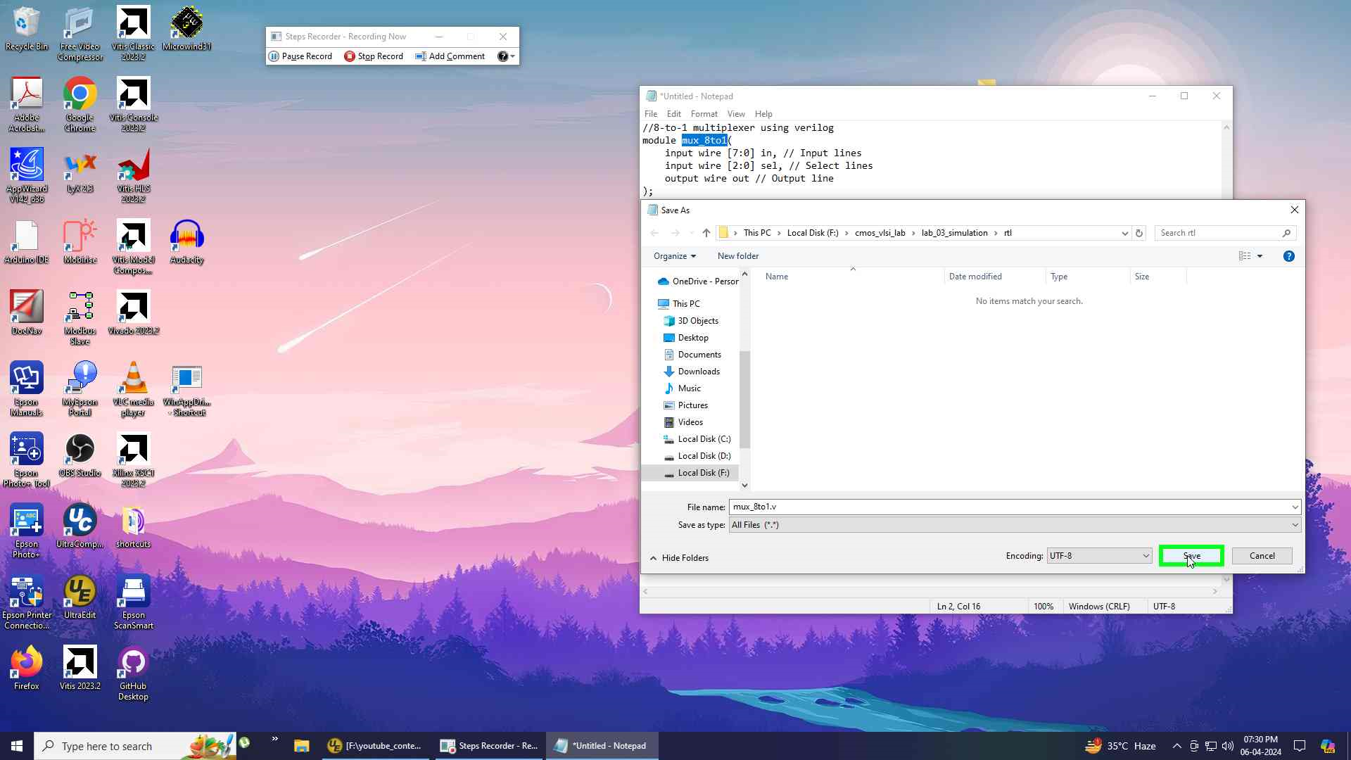
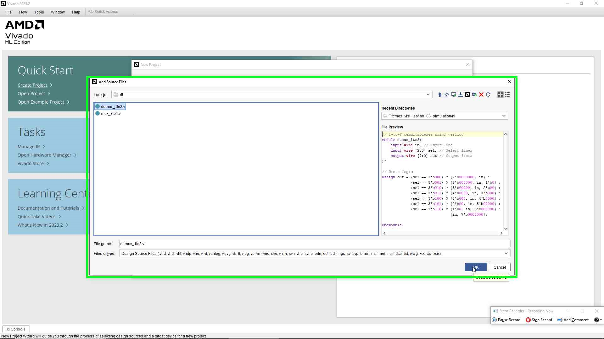
- Open Notepad or any text editor on a Windows machine and write the Verilog code for the 8-to-1 multiplexer and 1-to-8 demultiplexer.
- Save the files with a
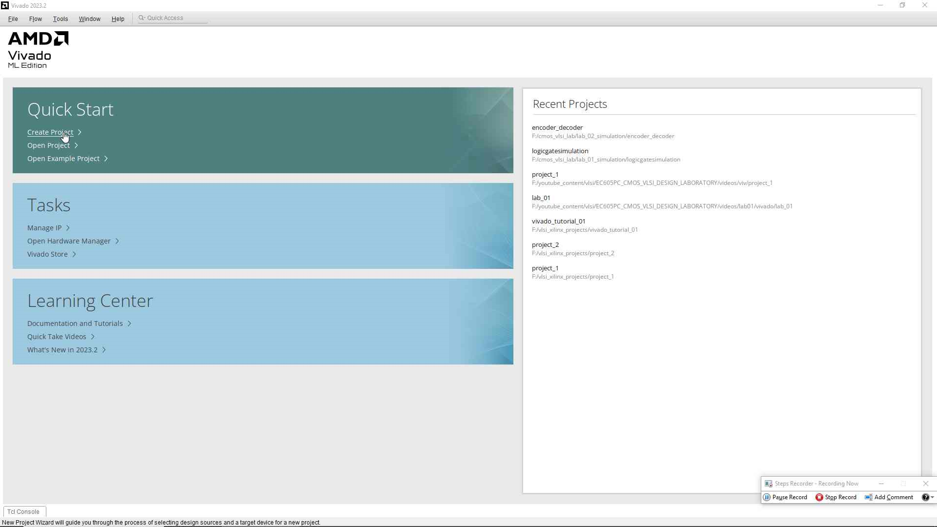
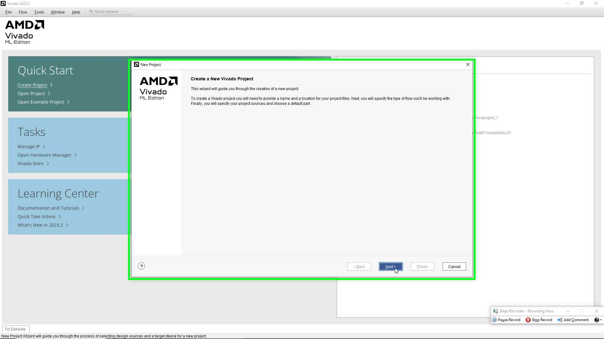
.vextension, selecting “All Files” as the save type. - Launch Xilinx Vivado from the desktop or start menu.
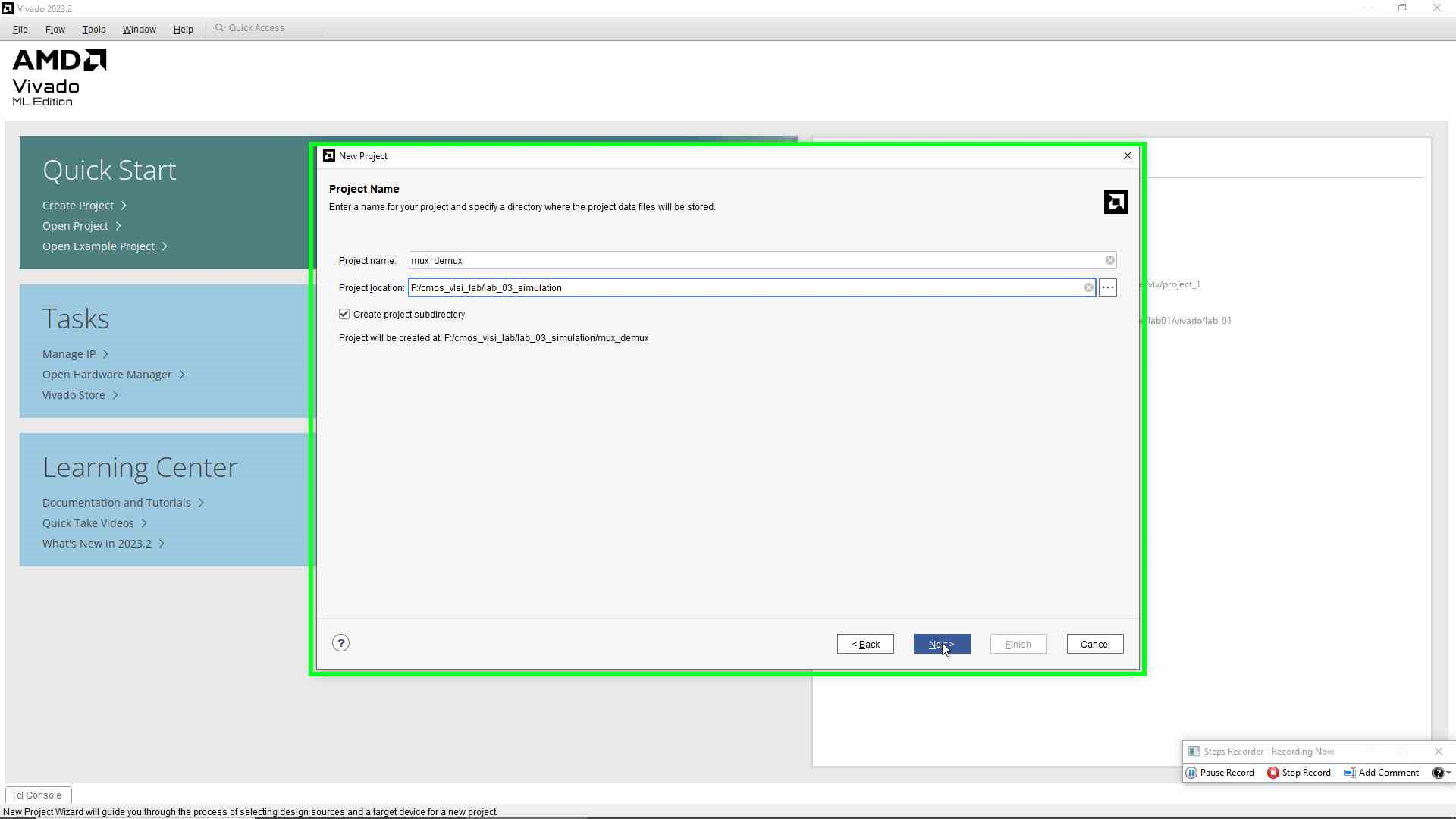
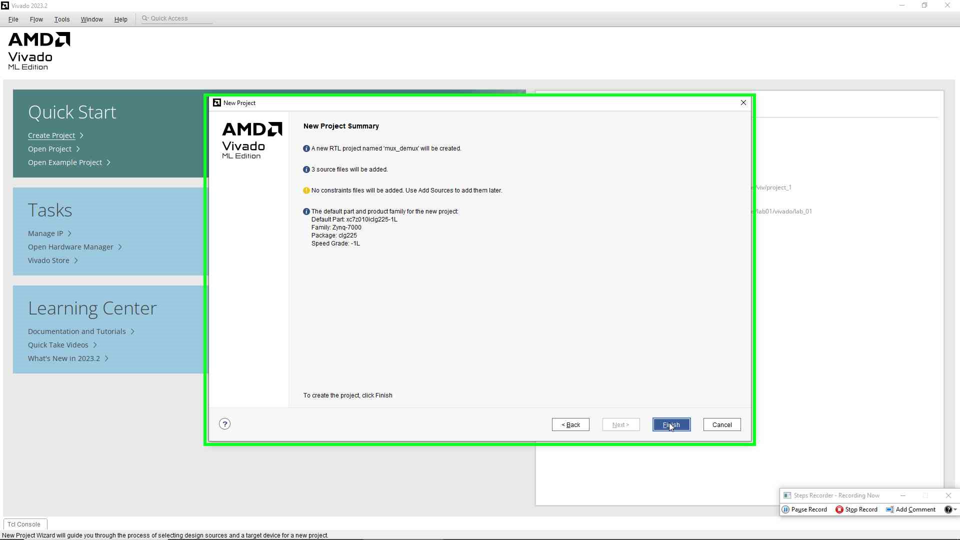
- Create a new project, naming it appropriately (e.g.,
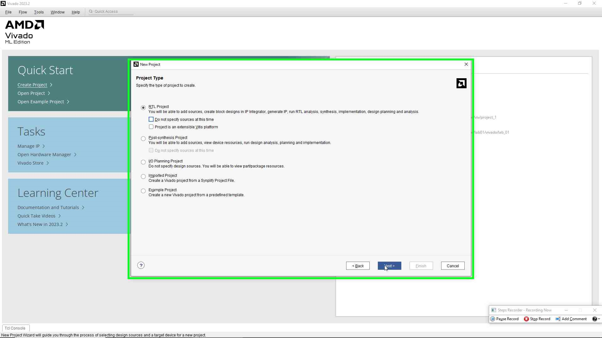
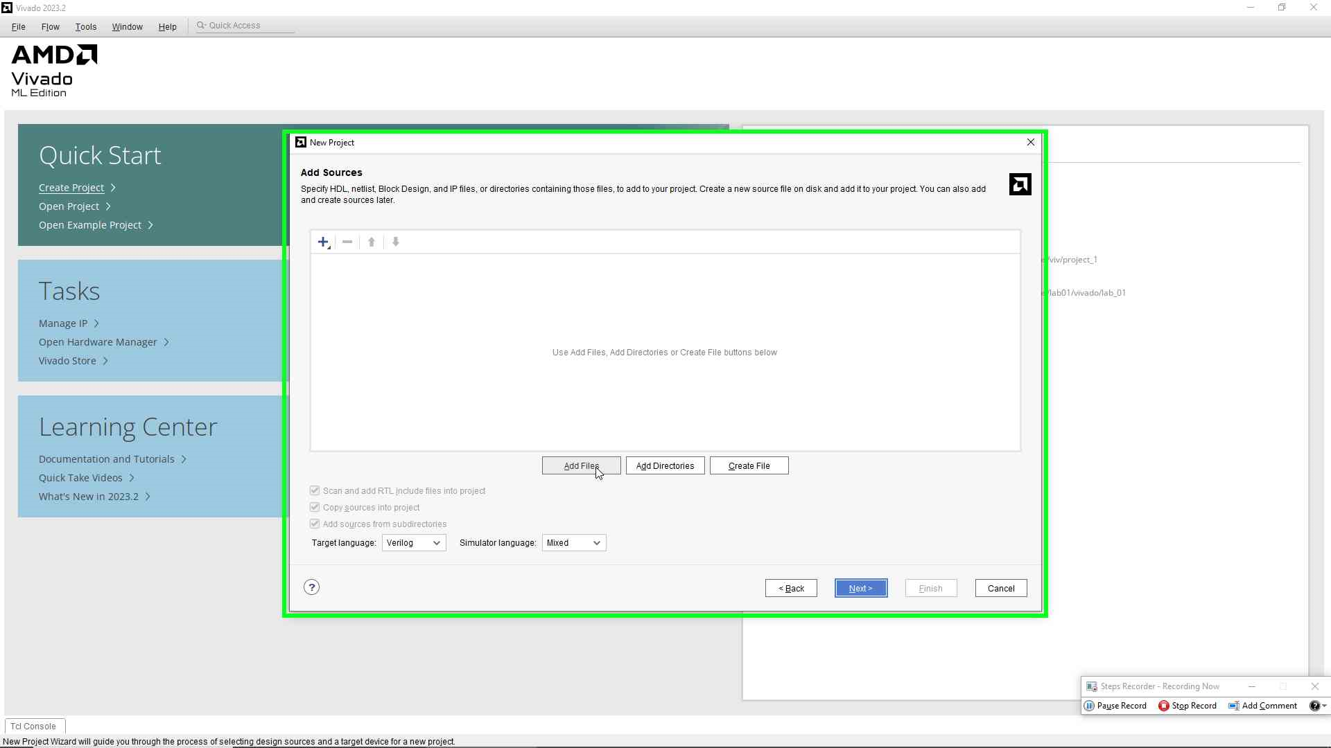
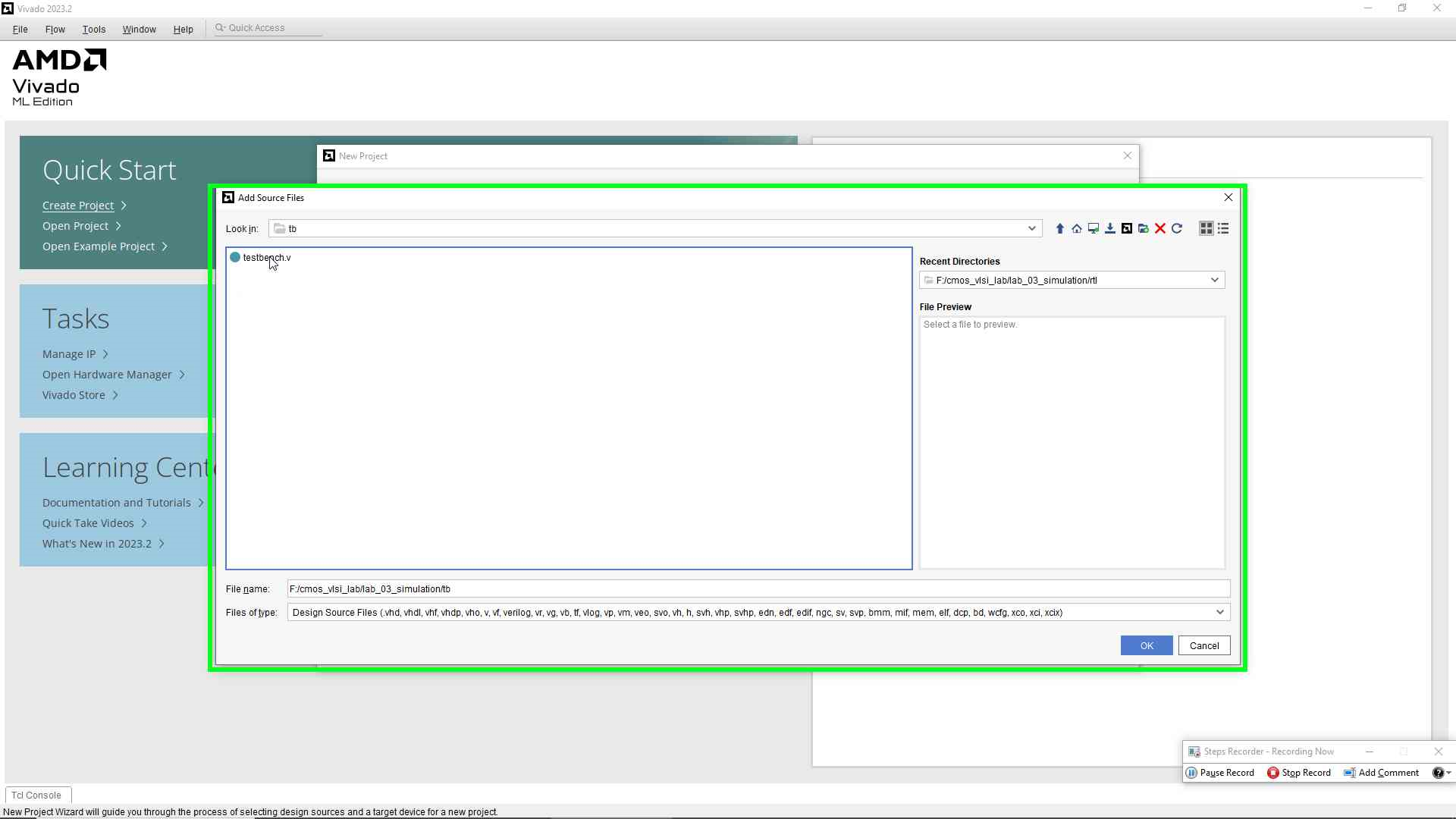
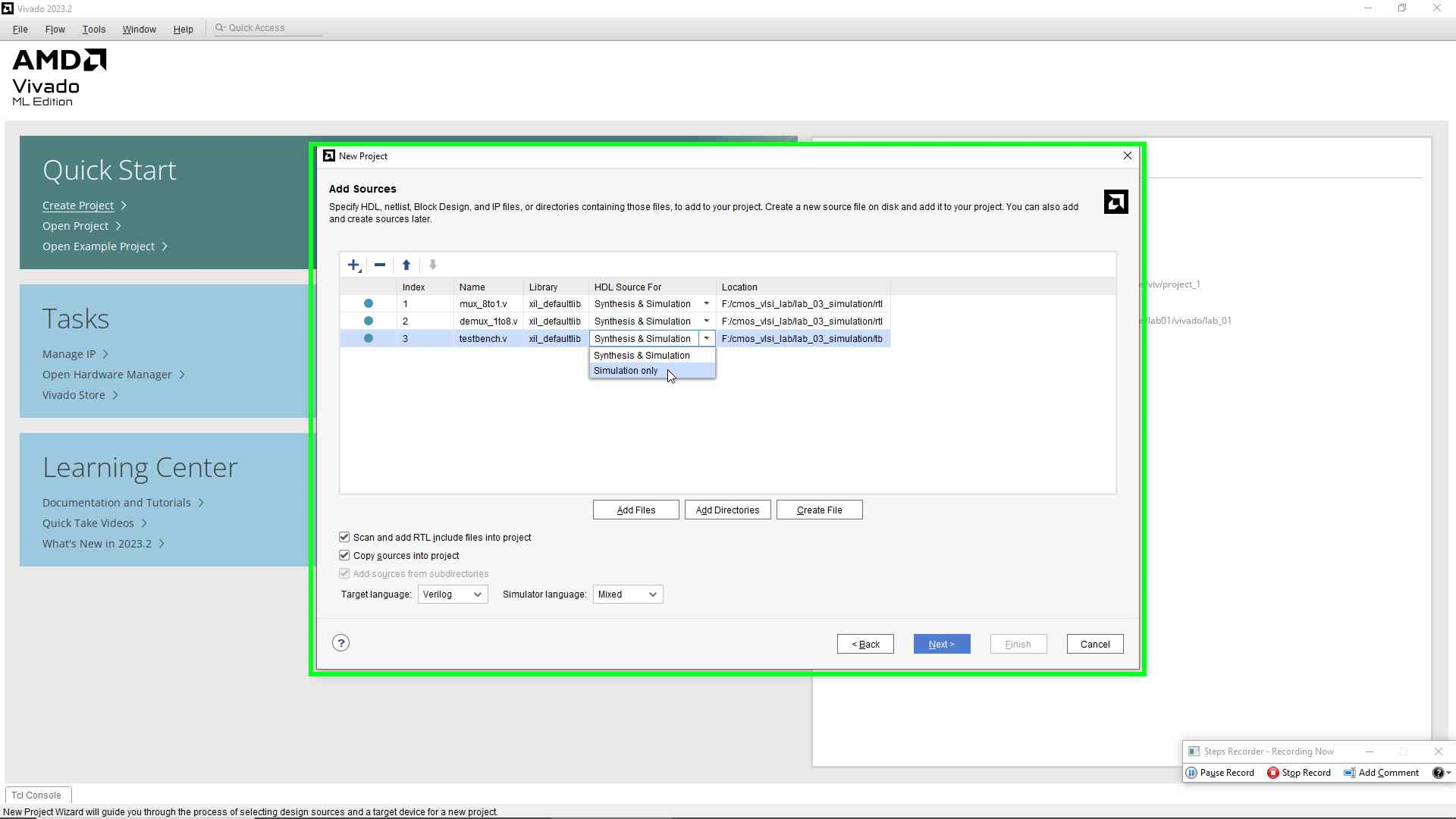
mux_demux_lab) and choosing the project’s storage location. - Ensure “RTL Project” is selected and specify sources at this time by pointing to the Verilog source code and testbench files you’ve created.
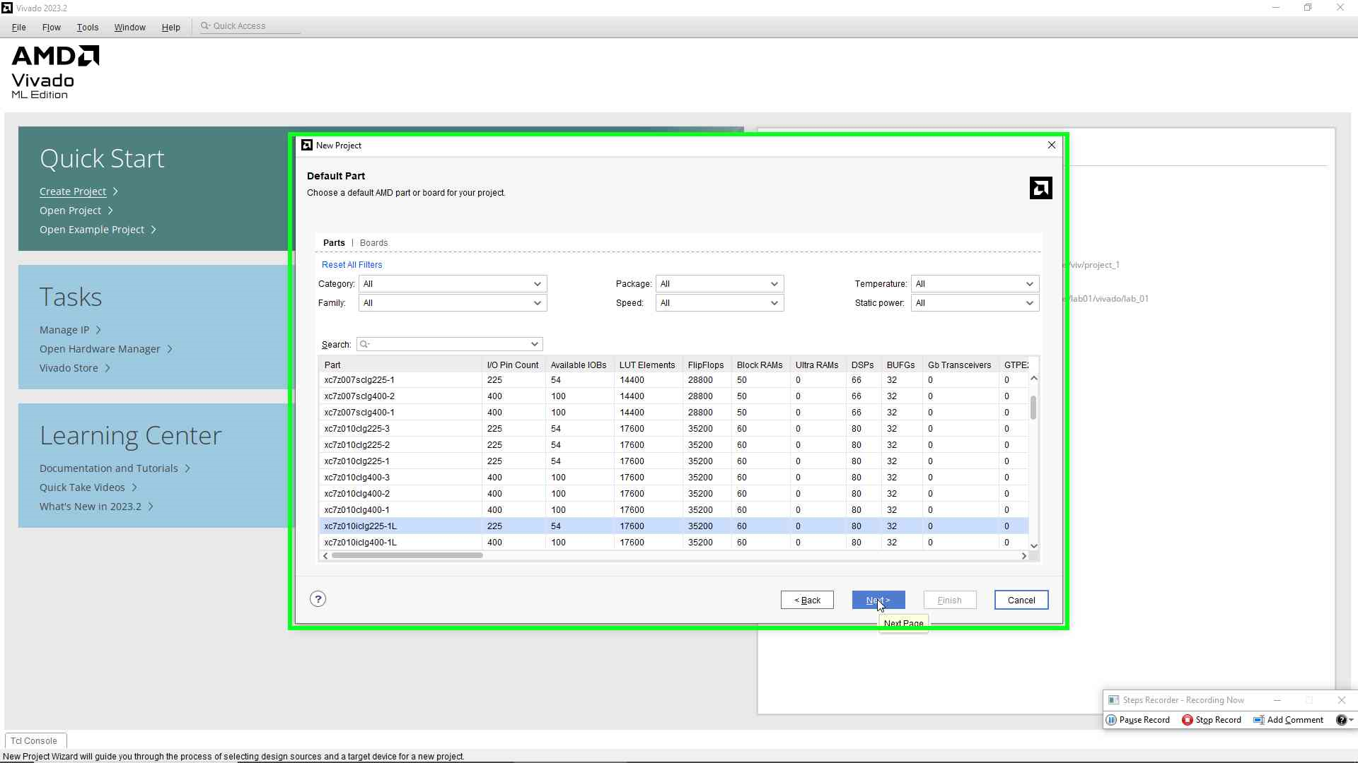
- Select the FPGA board or part targeted for this project using the search function.
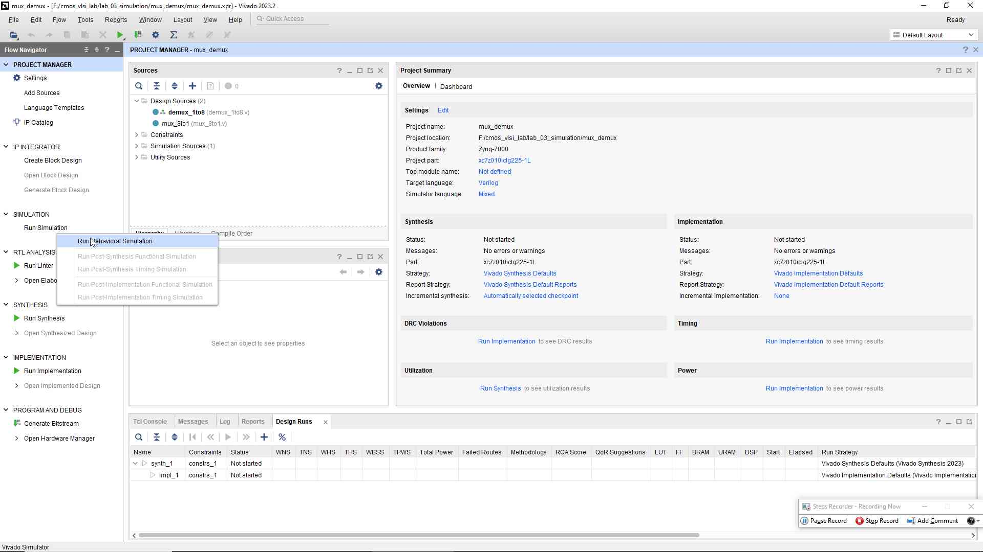
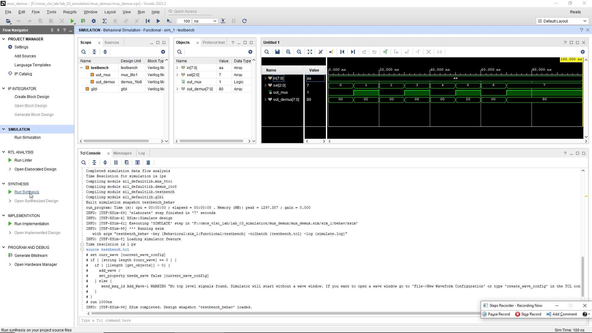
- Run Behavioral Simulation to compile the Verilog files and execute the simulation based on your testbench.
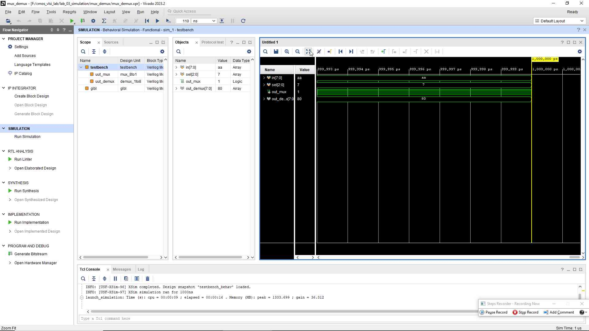
- Inspect the waveform viewer to verify that the outputs match the expected results based on your testbench scenarios.
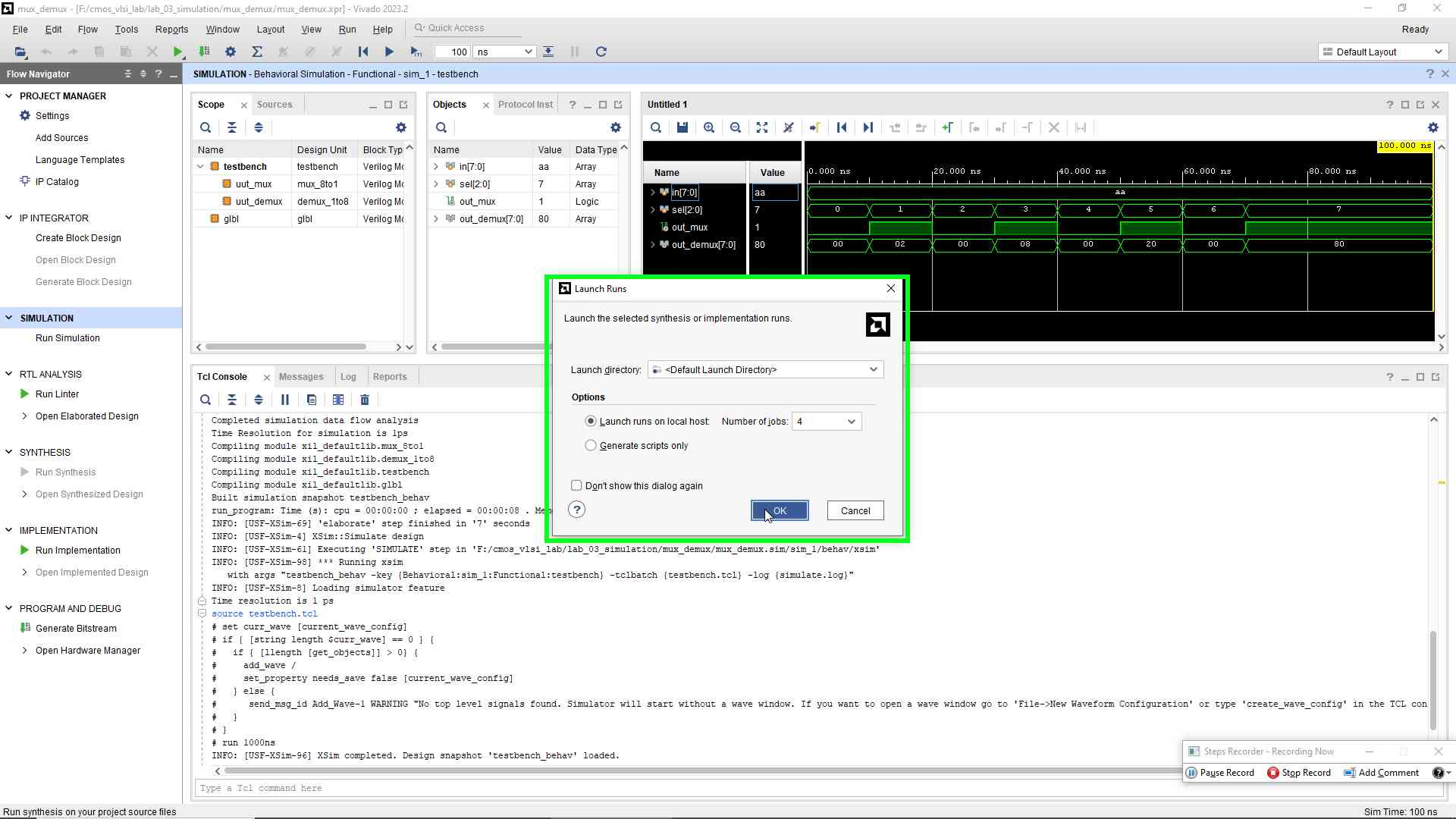
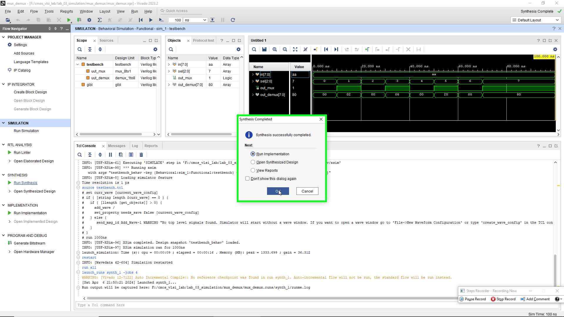
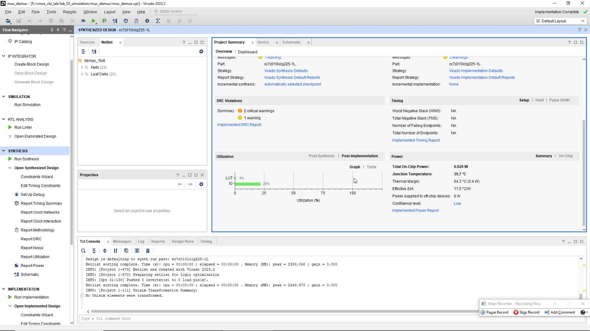
- Proceed with Synthesis and Implementation phases to optimize the design for performance and resource utilization.
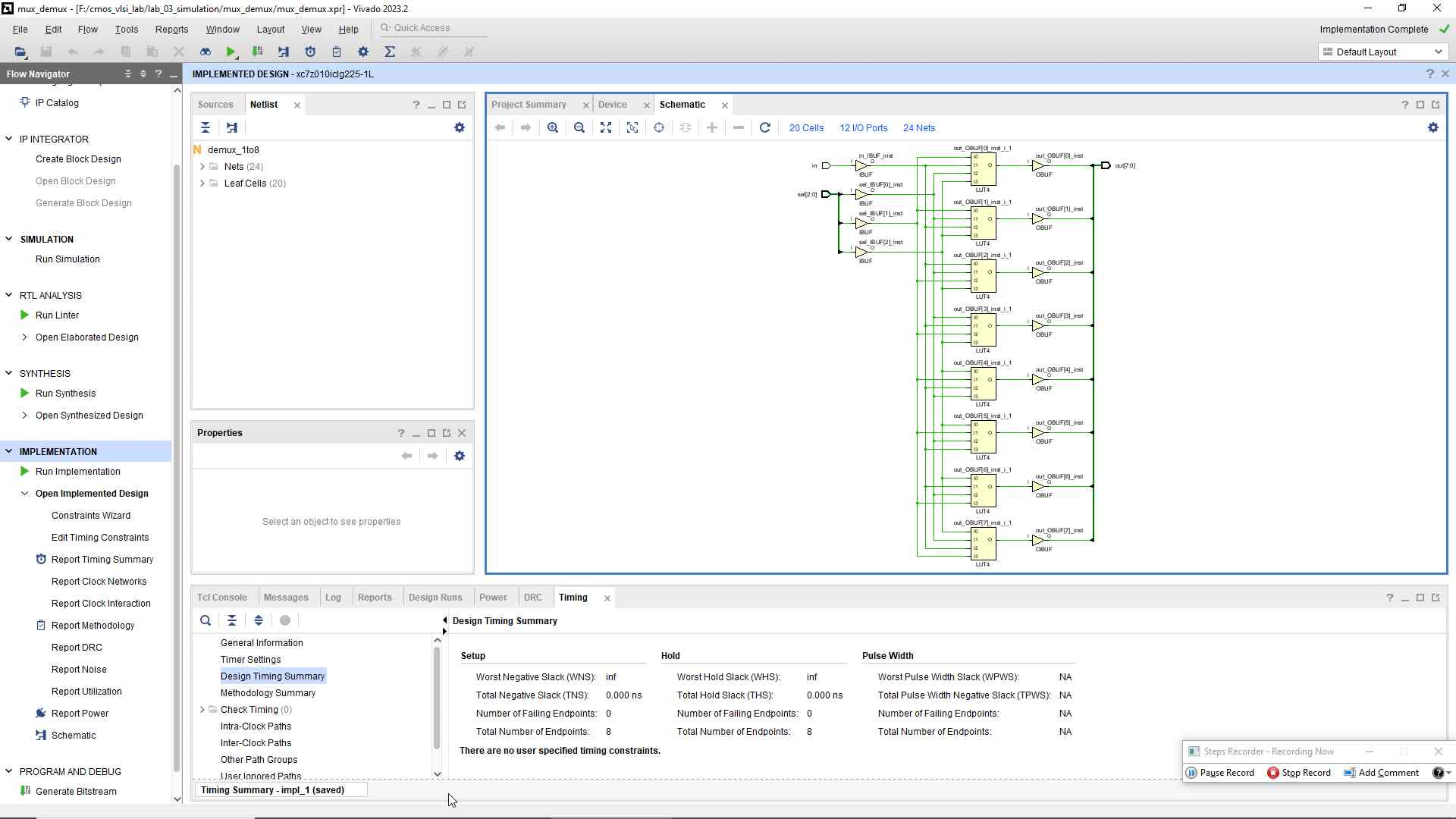
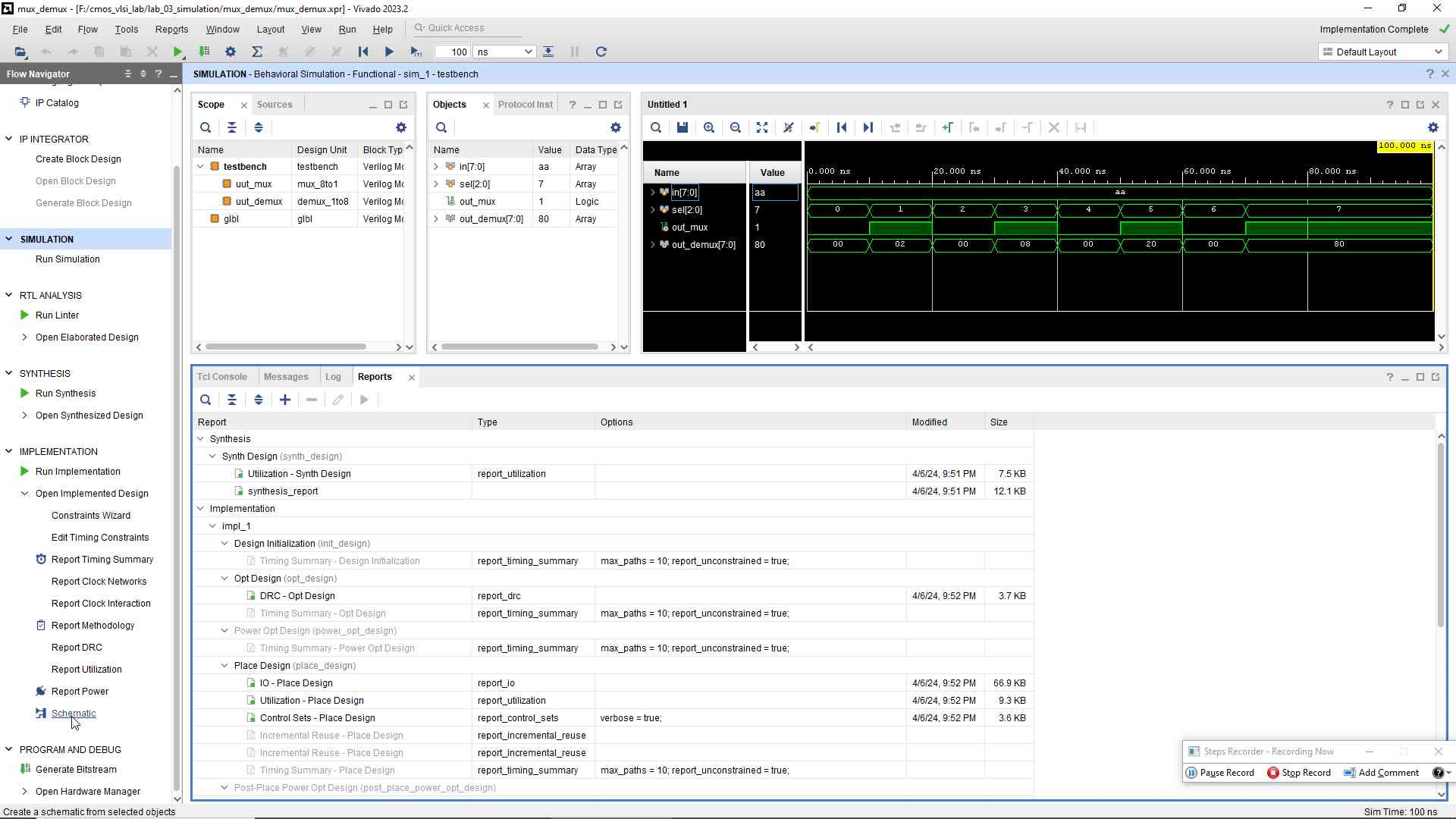
- Analyze the simulation results, synthesized schematic, and implementation reports, making necessary adjustments to refine your design.
Code
8-to-1 multiplexer using verilog
//8-to-1 multiplexer using verilog
module mux_8to1(
    input wire [7:0] in, // Input lines
    input wire [2:0] sel, // Select lines
    output wire out // Output line
);

// Mux logic
assign out = (sel == 3'b000) ? in[0] :
             (sel == 3'b001) ? in[1] :
             (sel == 3'b010) ? in[2] :
             (sel == 3'b011) ? in[3] :
             (sel == 3'b100) ? in[4] :
             (sel == 3'b101) ? in[5] :
             (sel == 3'b110) ? in[6] :
                               in[7];

endmodule
1-to-8 demultiplexer using verilog
// 1-to-8 demultiplexer using verilog
module demux_1to8(
    input wire in, // Input line
    input wire [2:0] sel, // Select lines
    output wire [7:0] out // Output lines
);

// Demux logic
assign out = (sel == 3'b000) ? {7'b0000000, in} :
             (sel == 3'b001) ? {6'b000000, in, 1'b0} :
             (sel == 3'b010) ? {5'b00000, in, 2'b00} :
             (sel == 3'b011) ? {4'b0000, in, 3'b000} :
             (sel == 3'b100) ? {3'b000, in, 4'b0000} :
             (sel == 3'b101) ? {2'b00, in, 5'b00000} :
             (sel == 3'b110) ? {1'b0, in, 6'b000000} :
                               {in, 7'b0000000};

endmodule
Testbench
// Testbench for 8-to-1 multiplexer and 1-to-8 demultiplexer
`timescale 1ns / 1ps
module testbench;

// Test signals
reg [7:0] in;
reg [2:0] sel;
wire out_mux;
wire [7:0] out_demux;

// Instantiate the Unit Under Test (UUT)
mux_8to1 uut_mux(
    .in(in),
    .sel(sel),
    .out(out_mux)
);

demux_1to8 uut_demux(
    .in(out_mux),
    .sel(sel),
    .out(out_demux)
);

initial begin
    // Initialize Inputs
    in = 8'b10101010;
    sel = 0;

    // Wait 10 ns for global reset to finish
    #10;

    // Add stimulus here
    sel = 3'b001; #10;
    sel = 3'b010; #10;
    sel = 3'b011; #10;
    sel = 3'b100; #10;
    sel = 3'b101; #10;
    sel = 3'b110; #10;
    sel = 3'b111; #10;
end

endmodule
Results:
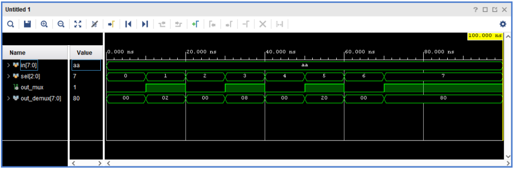
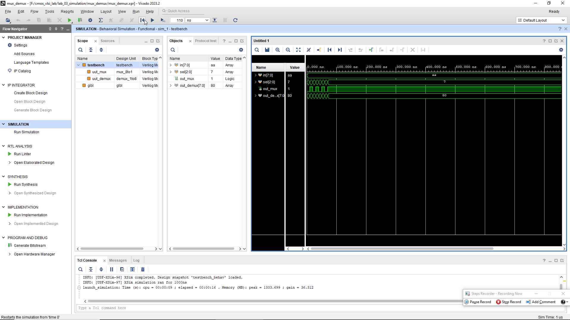
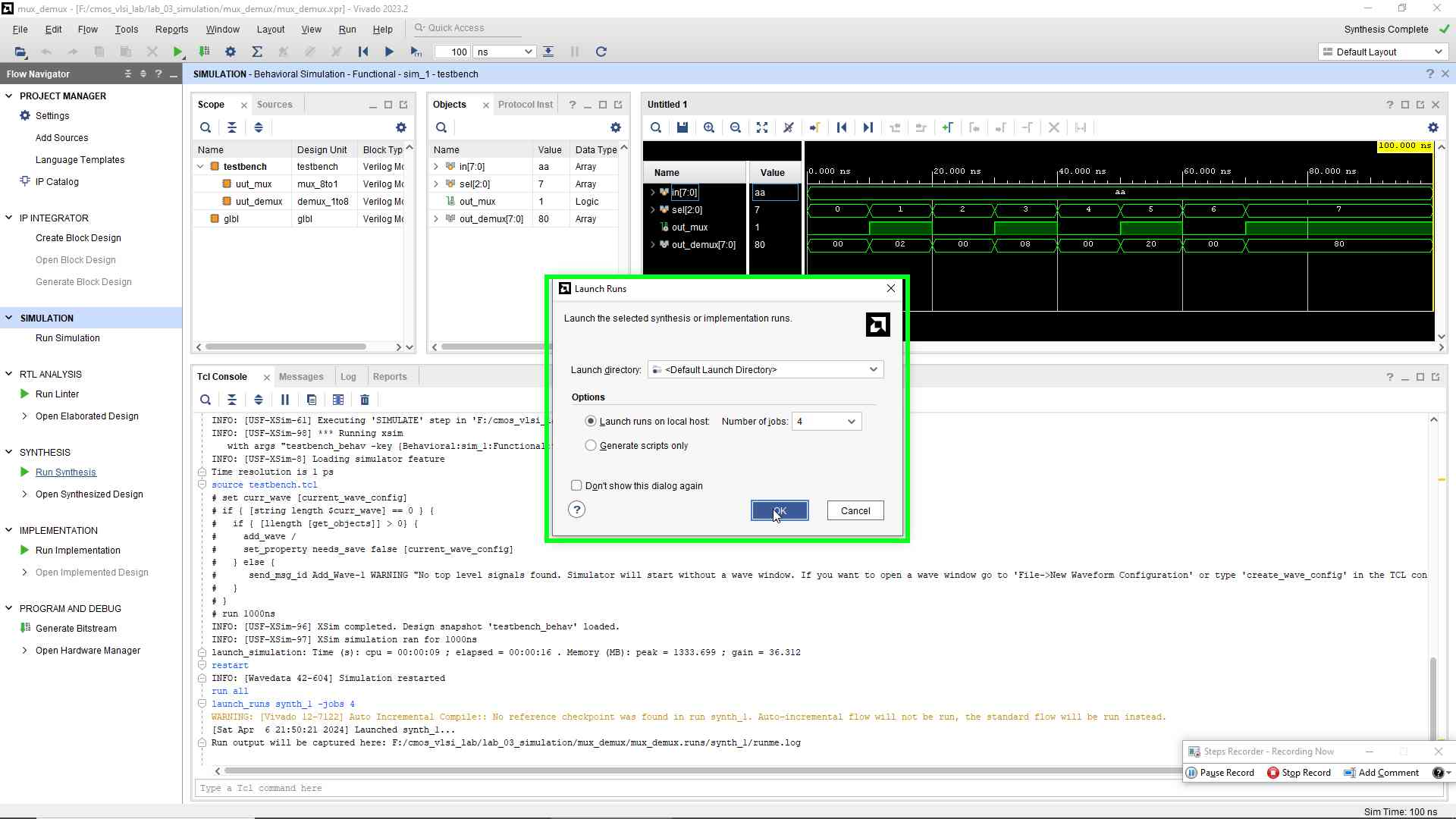
After following the steps correctly, the simulation in Xilinx Vivado will show the expected behavior for both the 8-to-1 multiplexer and 1-to-8 demultiplexer, aligning with the input and output relations defined in the theory section.
Detailed Inputs and Outputs Table
| in7 | in6 | in5 | in4 | in3 | in2 | in1 | in0 | sel2 | sel1 | sel0 | Expected out_mux | out_demux7 | out_demux6 | out_demux5 | out_demux4 | out_demux3 | out_demux2 | out_demux1 | out_demux0 |
|---|---|---|---|---|---|---|---|---|---|---|---|---|---|---|---|---|---|---|---|
| 1 | 0 | 1 | 0 | 1 | 0 | 1 | 0 | 0 | 0 | 0 | 1 | 1 | 0 | 0 | 0 | 0 | 0 | 0 | 0 |
| 1 | 0 | 1 | 0 | 1 | 0 | 1 | 0 | 0 | 0 | 1 | 0 | 0 | 1 | 0 | 0 | 0 | 0 | 0 | 0 |
| 1 | 0 | 1 | 0 | 1 | 0 | 1 | 0 | 0 | 1 | 0 | 1 | 0 | 0 | 1 | 0 | 0 | 0 | 0 | 0 |
| 1 | 0 | 1 | 0 | 1 | 0 | 1 | 0 | 0 | 1 | 1 | 0 | 0 | 0 | 0 | 1 | 0 | 0 | 0 | 0 |
| 1 | 0 | 1 | 0 | 1 | 0 | 1 | 0 | 1 | 0 | 0 | 1 | 0 | 0 | 0 | 0 | 1 | 0 | 0 | 0 |
| 1 | 0 | 1 | 0 | 1 | 0 | 1 | 0 | 1 | 0 | 1 | 0 | 0 | 0 | 0 | 0 | 0 | 1 | 0 | 0 |
| 1 | 0 | 1 | 0 | 1 | 0 | 1 | 0 | 1 | 1 | 0 | 1 | 0 | 0 | 0 | 0 | 0 | 0 | 1 | 0 |
| 1 | 0 | 1 | 0 | 1 | 0 | 1 | 0 | 1 | 1 | 1 | 0 | 0 | 0 | 0 | 0 | 0 | 0 | 0 | 1 |
- Input Bits (
in7toin0): Represent an 8-bit binary value10101010applied to the MUX. - Select Lines (
sel2,sel1,sel0):- Determine which of the eight input bits is selected by the MUX and which output bit is activated by the DEMUX.
- The binary combination of these lines directly corresponds to the bit positions
0to7.
- Expected out_mux:
- Shows the bit from the selected input (
in7toin0) by the MUX, based onsellines.
- Shows the bit from the selected input (
- Output Bits of DEMUX (
out_demux7toout_demux0):- Indicate which output bit is
high(1) based on thesellines and the input fromout_mux. - Only one of these outputs will be
highat any time, corresponding to thesellines’ binary value.
- Indicate which output bit is
- Selection and Output Relationship:
- When
selis000,sel2=0,sel1=0,sel0=0, the MUX selectsin0, makingout_muxandout_demux0high. - This pattern continues, with the select lines (
sel2,sel1,sel0) incrementing to choose subsequent input bits and direct the corresponding DEMUX output tohigh.
- When
Conclusion:
This lab experiment solidifies the understanding and application of multiplexers and demultiplexers in digital design, showcasing the practical use of Xilinx Vivado in simulating complex VLSI components.
Viva-Voce Questions:
- What is a multiplexer?
A multiplexer is a device that selects one of many input signals and forwards the selected input into a single line. - Define a demultiplexer.
A demultiplexer takes a single input signal and selects one of many output lines to send it to. - What are the uses of multiplexers and demultiplexers in digital circuits?
They are used for data routing, signal selection, and reducing the number of wires needed to connect systems. - How does a 1-to-8 demultiplexer work.
It takes a single input and routes it to one of the 8 outputs based on the 3-bit select line. - What is the importance of testbenches in Verilog?
Testbenches are crucial for verifying the functionality of Verilog modules by simulating input signals and observing the outputs. - How do you select the FPGA board in Vivado?
Within Vivado, you select the FPGA board by navigating to the ‘Default Part’ screen during project creation and using filters or the search function. - What is the role of synthesis in the Vivado Design Suite?
Synthesis transforms high-level design descriptions into gate-level representations, optimizing for performance and resource utilization. - Explain the implementation process in Vivado.
Implementation involves placement and routing, converting the synthesized design into a layout specific to the target FPGA device. - Why is it important to review synthesized schematics and implementation reports?
Reviewing these allows designers to ensure the design meets specifications, optimizes resource usage, and adheres to timing constraints. - How can one optimize a VLSI design for performance and efficiency?
By analyzing and refining based on synthesis and implementation reports, focusing on reducing complexity, and meeting timing and power consumption goals.
Complete Detailed Procedure for Simulation in Xilinx Vivado
- Preparation: Before opening Vivado, ensure all Verilog source files and testbenches are correctly written and saved.


- Project Creation: Launch Vivado, create a new project, and specify your project’s name and location.
- Adding Files: Include your Verilog source and testbench files in the project setup.
- Selecting Target Device: Choose the FPGA board or part you’re targeting, based on your project requirements.
- Running Simulation: Utilize the Behavioral Simulation feature to compile and simulate your Verilog files.

- Synthesis and Implementation: After verifying the simulation results, proceed with synthesis and implementation to optimize your design.

- Analysis: Review synthesized schematics, implementation reports, and simulation results to ensure the design meets all criteria.

- Adjustments and Finalization: Make any necessary design adjustments based on your analyses and save your project.
Additional Reading:
- FPGA Design Fundamentals
- Verilog for Beginners
- Advanced Digital Design with the Verilog HDL
FAQ
- What is Xilinx Vivado?
Vivado is a software suite by Xilinx for synthesis and analysis of HDL designs, focusing on FPGA and SoC development. - Can I simulate non-Xilinx devices in Vivado?
Vivado is primarily designed for Xilinx devices, though generic Verilog/VHDL simulation is possible. - How do I debug in Vivado?
Use the integrated waveform viewer and debug tools for real-time analysis and troubleshooting. - What are the system requirements for Vivado?
Vivado requires a Windows or Linux OS, with specific memory, processor, and storage requirements detailed on Xilinx’s website. - Where can I learn more about VLSI design using Vivado?
Xilinx provides extensive documentation, tutorials, and community forums for learning Vivado and VLSI design.
Reference:
- Official Xilinx Vivado Documentation
- Digital Design and Computer Architecture by Harris & Harris
- FPGA Prototyping by Verilog Examples by Pong P. Chu
Internal links:
External Links: