Introduction to Creating a 4-Input AND-OR-NOT Complex Gate Layout using Vivado and Microwind
Welcome to the exciting world of CMOS VLSI Design! If you’re a B.Tech student in your third year, second semester, enrolled in the “CMOS VLSI Design Laboratory” course at JTUH, you’re about to embark on a fascinating journey. This blog aims to guide you through the process of designing a 4-input AND/OR/NOT complex gate using two powerful tools: Vivado and Microwind.
What You’ll Learn
In this lab, you’ll get hands-on experience with:
- Vivado: A state-of-the-art design suite from Xilinx, which is widely used for HDL design, simulation, and synthesis.
- Microwind: A comprehensive tool for designing and simulating integrated circuits at the physical layout level.
Why These Tools?
- Vivado: Known for its robust support for HDL (Hardware Description Language) designs, Vivado helps you create and test your digital logic circuits with precision.
- Microwind: Offers an intuitive interface for designing and simulating the physical layout of CMOS circuits, making it ideal for understanding the intricacies of VLSI design.
The 4-Input AND/OR/NOT Complex Gate
In this lab, we will focus on creating a complex gate that integrates 4-input AND, OR, and NOT functionalities. This exercise will provide you with a deep understanding of both the logical design and the physical layout aspects of VLSI design.
Real-World Relevance
Understanding how to design and implement these basic logic gates is crucial for anyone looking to pursue a career in digital system design or embedded systems. These gates form the building blocks of more complex circuits used in everything from microprocessors to advanced embedded systems.
The Process
We’ll break down the entire process into manageable steps:
- Designing the Logic: Using Vivado to create the HDL description of the 4-input complex gate.
- Simulating the Logic: Testing the design within Vivado to ensure it performs as expected.
- Layout Design: Transferring the HDL design into Microwind to create the physical layout.
- Layout Simulation: Simulating the physical layout in Microwind to verify its functionality.
By the end of this lab, you will have a solid understanding of how to design, simulate, and implement a complex gate, both logically and physically. Let’s dive in and start creating!
Lab Report
AIM: Layout Design and Simulation of Latch
Apparatus / Software required
- Windows Machine with Xilinx Vivado and Microwind Software Installed
Theory
Understanding AOI Logic
AOI (AND-OR-INVERT) logic is a fundamental concept in digital design. It combines the basic operations of AND, OR, and NOT gates to create more complex logic functions. The specific AOI logic we’ll be focusing on in this lab is represented by the equation:
Y=(AB+CD)’
In this equation:
- (A) and (B) are the inputs to the first AND gate.
- (C) and (D) are the inputs to the second AND gate.
- The outputs of these two AND gates are then OR-ed together.
- Finally, the result of the OR operation is inverted to produce the final output, (Y).
Truth Table for AOI Logic
To understand how this logic works, let’s examine the truth table. The table below shows all possible input combinations and their corresponding output for the given AOI logic.
Here is the truth table for the AOI logic represented by the equation ( \text{aoi_out} = \sim((a & b) | (c & d)) ):
| a | b | c | d | (a & b) | (c & d) | ((a & b) | (c & d)) | Y = ~((a & b) | (c & d)) |
|---|---|---|---|---|---|---|---|
| 0 | 0 | 0 | 0 | 0 | 0 | 0 | 1 |
| 0 | 0 | 0 | 1 | 0 | 0 | 0 | 1 |
| 0 | 0 | 1 | 0 | 0 | 0 | 0 | 1 |
| 0 | 0 | 1 | 1 | 0 | 1 | 1 | 0 |
| 0 | 1 | 0 | 0 | 0 | 0 | 0 | 1 |
| 0 | 1 | 0 | 1 | 0 | 0 | 0 | 1 |
| 0 | 1 | 1 | 0 | 0 | 0 | 0 | 1 |
| 0 | 1 | 1 | 1 | 0 | 1 | 1 | 0 |
| 1 | 0 | 0 | 0 | 0 | 0 | 0 | 1 |
| 1 | 0 | 0 | 1 | 0 | 0 | 0 | 1 |
| 1 | 0 | 1 | 0 | 0 | 0 | 0 | 1 |
| 1 | 0 | 1 | 1 | 0 | 1 | 1 | 0 |
| 1 | 1 | 0 | 0 | 1 | 0 | 1 | 0 |
| 1 | 1 | 0 | 1 | 1 | 0 | 1 | 0 |
| 1 | 1 | 1 | 0 | 1 | 0 | 1 | 0 |
| 1 | 1 | 1 | 1 | 1 | 1 | 1 | 0 |
Procedure
Pat – 1: Design and Simulation using Vivado
- Open Notepad or any text editor on a Windows machine and write the Verilog code for 4 input AND-OR-Invert logic using Structural modeling and corresponding testbench.
- Save the files with a
.vextension, selecting “All Files” as the save type. - Launch Xilinx Vivado from the desktop or start menu.
- Create a new project, naming it appropriately (e.g.,
aio_4_lab12) and choosing the project’s storage location. - Ensure “RTL Project” is selected and specify sources at this time by pointing to the Verilog source code and testbench files you’ve created.
- Select the FPGA board or part targeted for this project using the search function.
- Run Behavioral Simulation to compile the Verilog files and execute the simulation based on your testbench.
- Inspect the waveform viewer to verify that the outputs match the expected results based on your testbench scenarios.
- Proceed with Synthesis and Implementation phases to optimize the design for performance and resource utilization.
- Analyze the simulation results, synthesized schematic, and implementation reports, making necessary adjustments to refine your design.
Pat – 2: Layout Design and Simulation using Vivado
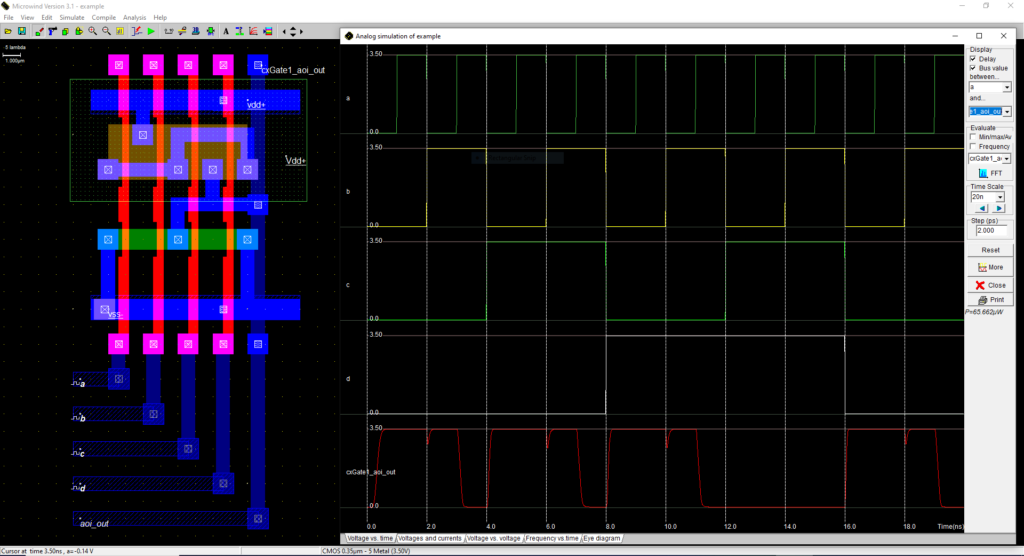
- Open Microwind, select the 0.35 micrometer foundry under the file tab, and compile the Verilog file using the ‘compile Verilog’ option.
- Complete the layout by arranging metal layers and connections, add a VDD connection to the N-well region.
- Run the layout simulation to verify output behavior with varying enable signals and observe frequency and power consumption by using the respective simulation tools.
- Save the final layout as ‘aoi_gate_v01.msk’ for future reference.
- Ensure all settings and simulations are accurately documented and adjusted as necessary for complete verification of the AOI design.
Code
AOI RTL Verilog Code
module aoi_gate(
    input wire a,
    input wire b,
    input wire c,
    input wire d,
    output wire aoi_out
);

    // implement the aoi logic
    assign aoi_out = ~((a & b) | (c & d));

endmodule
// Simulation parameters
// a CLK 10.000 10.000
// b CLK 20.000 20.000
// c CLK 40.000 40.000
// d CLK 80.000 80.000
Testbench Verilog Code
`timescale 1ns / 1ps

module tb_aoi_4_lab12_v01;

    // Inputs
    reg a;
    reg b;
    reg c;
    reg d;

    // Output
    wire aoi_out;

    // Instantiate the Unit Under Test (UUT)
    aoi_gate uut (
        .a(a),
        .b(b),
        .c(c),
        .d(d),
        .aoi_out(aoi_out)
    );

    // Clock generation for inputs a, b, c, and d
    initial begin
        a = 0;
        b = 0;
        c = 0;
        d = 0;
    end

    always #80 a = ~a;  // toggle 'a' every 80 time units
    always #40 b = ~b;  // toggle 'b' every 40 time units
    always #20 c = ~c;  // toggle 'c' every 20 time units
    always #10 d = ~d;  // toggle 'd' every 10 time units

endmodule
Results
After following the steps correctly, the simulation in Microwind show the expected behavior for AOI gate, aligning with the input and output relations defined in the theory section.
Conclusion
The experiment successfully demonstrates the practical application of schematic to layout conversion for complex designs using Xilinx Vivado and Microwind.
Viva-Voce Questions
Certainly! Below are 20 viva voce questions designed for a practical related to the CMOS schematic of a AND-OR-INVERTHere are 20 viva voce questions related to the process of creating the layout of a 4-input AND-OR-NOT complex gate using Vivado in Verilog and then creating its layout using Microwind:
Q1: What is the purpose of using Verilog in VLSI design?
- Verilog is used for modeling electronic systems, enabling the design and verification of digital circuits at various abstraction levels.
Q2: What is Vivado, and how is it used in VLSI design?
- Vivado is an integrated design environment (IDE) developed by Xilinx for FPGA and SoC design, used for synthesis, simulation, and implementation of digital circuits.
Q3: What are the primary steps involved in designing a 4-input AND-OR-NOT complex gate in Verilog?
- The primary steps include writing the Verilog code for the gate, synthesizing the code, simulating the design, and generating the netlist.
Q4: How do you declare a module in Verilog for a 4-input AND-OR-NOT complex gate?
- A module is declared using the
modulekeyword followed by the module name, input and output ports.
Q5: What is the significance of using the always block in Verilog?
- The
alwaysblock is used to describe the behavior of sequential circuits, specifying actions that should occur on changes to specified signals.
Q6: How do you perform synthesis in Vivado for a Verilog module?
- Synthesis is performed by using the synthesis tool in Vivado, which translates the Verilog code into a gate-level netlist.
Q7: What is a netlist, and why is it important?
- A netlist is a description of the connectivity of an electronic circuit, crucial for the subsequent stages of physical design and verification.
Q8: What is the role of testbenches in Verilog?
- Testbenches are used to simulate and verify the functionality of Verilog modules by applying stimulus and checking the output.
Q9: How do you define inputs and outputs in a Verilog module?
- Inputs and outputs are defined using the
inputandoutputkeywords, respectively, followed by the signal names.
Q10: What are the key differences between behavioral and structural modeling in Verilog?
- Behavioral modeling describes what a circuit does, while structural modeling describes how a circuit is constructed using gates and interconnections.
Q11: What is Microwind, and how is it used in VLSI design?
- Microwind is a tool for designing and simulating the physical layout of VLSI circuits, converting netlists into layout designs.
Q12: How do you import a netlist into Microwind?
- A netlist can be imported into Microwind by using the appropriate import function, which translates the netlist into a layout design.
Q13: What are the main steps in creating a layout in Microwind?
- The main steps include importing the netlist, placing the components, routing the interconnections, and verifying the layout.
Q14: What is the purpose of Design Rule Check (DRC) in Microwind?
- DRC ensures that the layout adheres to the fabrication process constraints, checking for spacing, width, and other design rules.
Q15: How does the AND-OR-NOT complex gate function in digital logic?
- The AND-OR-NOT gate performs a combination of logical AND, OR, and NOT operations on its inputs to produce an output.
Q16: Why is layout design crucial in VLSI?
- Layout design determines the physical implementation of the circuit on silicon, impacting performance, power consumption, and area.
Q17: What is LVS (Layout vs. Schematic) check, and why is it performed?
- LVS compares the layout with the original schematic/netlist to ensure they match, verifying the correctness of the layout.
Q18: How do you optimize the layout for performance and area in Microwind?
- Optimization involves careful placement of components, efficient routing, and minimizing parasitic effects to enhance performance and reduce area.
Q19: What are parasitic effects in VLSI design, and how do they impact circuit performance?
- Parasitic effects include unwanted resistances, capacitances, and inductances in the layout, affecting signal integrity and circuit speed.
Q20: How can power consumption be minimized in a VLSI layout?
- Power consumption can be minimized by using low-power design techniques, optimizing the layout for minimal switching activity, and reducing leakage currents.
FAQ
Here are 10 frequently asked questions (FAQs) related to the process of creating the layout of a 4-input AND-OR-NOT complex gate using Vivado in Verilog and then creating its layout using Microwind:
Q1: What is the primary purpose of using Verilog in VLSI design?
- Verilog is used for describing electronic systems and designing digital circuits at various levels of abstraction, facilitating simulation and synthesis.
Q2: How does Vivado assist in the VLSI design process?
- Vivado provides an integrated environment for synthesizing, simulating, and implementing digital designs on FPGAs and SoCs.
Q3: What is the function of an AND-OR-NOT complex gate in digital logic?
- The AND-OR-NOT gate performs combined logical AND, OR, and NOT operations on its inputs to generate a desired output.
Q4: What are the key steps to design a 4-input AND-OR-NOT complex gate in Verilog using Vivado?
- Write the Verilog code, synthesize the design, simulate the functionality, and generate the netlist.
Q5: How is a testbench used in Verilog?
- A testbench applies inputs to the design and checks the outputs to verify that the design behaves as expected.
Q6: What is the role of Microwind in VLSI layout design?
- Microwind is used for creating and simulating the physical layout of VLSI circuits, converting netlists into detailed layouts.
Q7: How do you import a Verilog netlist into Microwind for layout design?
- The netlist is imported into Microwind using the import function, which translates the design into a physical layout.
Q8: What is Design Rule Check (DRC), and why is it important?
- DRC ensures that the layout complies with fabrication process constraints, checking for design rule violations such as spacing and width.
Q9: How do you verify the correctness of the layout in Microwind?
- Use Layout vs. Schematic (LVS) checks to compare the layout with the original schematic or netlist, ensuring they match.
Q10: Why is it essential to optimize the layout for power, performance, and area?
- Optimizing the layout improves circuit efficiency by reducing power consumption, enhancing performance, and minimizing the area, which is crucial for cost-effective and high-speed designs.
Internal Links
- JNTUH VLSI Lab Experiments – Explore a series of lab experiments for understanding VLSI design concepts using Xilinx Vivado.
CMOS VLSI LAB CYCLE 01
Lab Reports and Related YouTube Videos
- Lab 01: Logic Gates
- Lab 02: Encoder and Decoder
- Lab 03: Multiplexer, Demultiplexer
- Lab 04: Binary to Gray Converter
- Lab 05: Comparator Circuit
- Lab 06: Adder Circuit
CMOS VLSI LAB CYCLE 02
Lab Reports and Related YouTube Video
- Lab 01 Part-2: Basic Logic Gates Layout
- Lab 02 Part-2: Inverter Layout
- Lab 03 Part-2: NOR and NAND gate design using Microwind
- Lab 04 Part-2: XOR gate and 2:1 Multiplexer design using Microwind
- Lab 05 Part-2: Latch design using Microwind
These resources provide a comprehensive overview and practical insights into various aspects of CMOS VLSI design, offering valuable information for students and enthusiasts interested in exploring the field of VLSI design using Xilinx Vivado and Microwind.