Introduction to Latch Layout Design in Micro Wind: A Practical Guide for CMOS VLSI Design Laboratory
Welcome to our deep dive into the intriguing world of VLSI (Very Large Scale Integration) design, specifically focusing on the creation of latch layouts using the Micro Wind software. This guide is tailored for students of the B.Tech III Year II Semester, enrolled in the CMOS VLSI Design Laboratory at JNTUH (Jawaharlal Nehru Technological University Hyderabad). Whether you’re a budding engineer eager to understand the nuances of VLSI design or an enthusiast looking to expand your knowledge, this blog is designed to provide you with a clear, practical perspective on the process.
VLSI technology has revolutionized the way electronic devices are manufactured, allowing millions of transistors to be integrated into a single chip. This leap in technology emphasizes not only miniaturization but also the efficiency and performance of integrated circuits (ICs). One fundamental component in these circuits is the latch, a type of memory cell that plays a critical role in storage and stability within digital systems.
In this blog, we’ll explore how to create a latch layout using Micro Wind, a popular software tool among VLSI designers for its user-friendly interface and powerful capabilities. The software facilitates the design and simulation of ICs at the micron and deep sub-micron levels, making it an excellent educational tool for understanding the practical aspects of chip design.
By the end of this article, you’ll gain insights into:
- The basic concepts of latch design and its importance in VLSI.
- Step-by-step instructions on how to layout a latch using Micro Wind.
- Best practices and tips to enhance your design skills in the CMOS VLSI Design Laboratory setting.
Let’s embark on this journey through the microscopic world of chips and circuits, transforming theoretical knowledge into practical skills that will shape your future in electronics and communication engineering.
Lab Report
AIM: Layout Design and Simulation of Latch
Apparatus / Software required:
- Windows Machine with Microwind Software Installed
Theory:
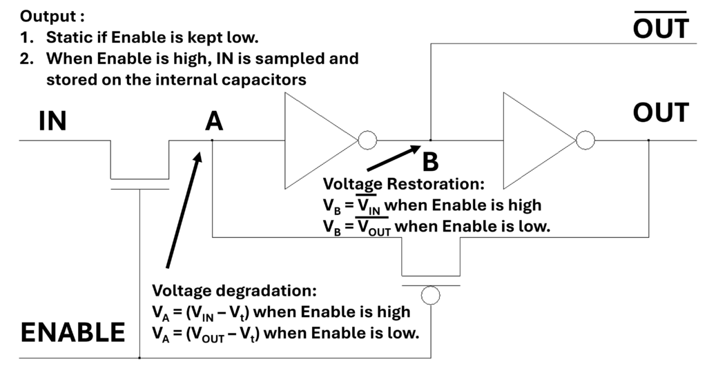
The latch design described involves a combination of inverter circuits and both NMOS and PMOS transistors. This type of configuration utilizes the basic properties of each component to create a stable memory device capable of maintaining a state until changed by inputs.
Inverters in the Latch Circuit
The latch utilizes two inverters connected in a feedback loop. Each inverter is responsible for ensuring that the output is the logical opposite of its input. In a typical latch configuration:
- The output of the first inverter feeds into the input of the second, and vice versa.
- This setup creates a feedback loop necessary for the latch to maintain its state either at logic high (1) or low (0).
NMOS and PMOS Transistors
The design incorporates both NMOS and PMOS transistors to control the flow of electricity based on the input signals:
- NMOS Transistor: Acts as a switch that closes (conducts) when a high voltage is applied to its gate (CLOCK in this case). When the CLOCK signal is high, and the data signal is also high, the NMOS transistor allows a connection between the input IN and node A, affecting the output states.
- PMOS Transistor: In contrast to the NMOS, the PMOS conducts when a low voltage is applied to its gate. This transistor connects the output node to node A when the CLOCK signal is low.
Functionality of the Latch
Combining these components, the latch operates as follows:
- When the CLOCK is high, the NMOS transistor checks the data input. If the data is high, the NMOS will conduct, pulling the node A to a weak High state (because the CLOCK input is high, which for NMOS means conductive state). This High state then passes on as high at the Q output due to two inverter.
- Simultaneously, if the CLOCK is low, the PMOS transistor conducts, ensuring that the node A is passed on a weak output state that is maintened by two inverters at the Q output.
This configuration allows the latch to store a bit of data (0 or 1), with the output Q showing the stored data and nQ showing its inverse. The use of both NMOS and PMOS transistors ensures that the circuit can respond appropriately to changes in the CLOCK and data signals, thus enabling the latch to switch states between set and reset conditions.
It should be noted that both PMOS and NMOS passes on input or output voltage to node A after a votge drop of threshod voltage VT. However due to two inverters this voltage drop is restored and the output swing is not affected.
Stability and Feedback
The critical aspect of this design is the feedback provided by connecting the output of one inverter to the input of another. This feedback loop ensures that once a state is set, it remains stable until an opposite input is provided, crucial for memory storage applications in digital electronics.
Procedure:
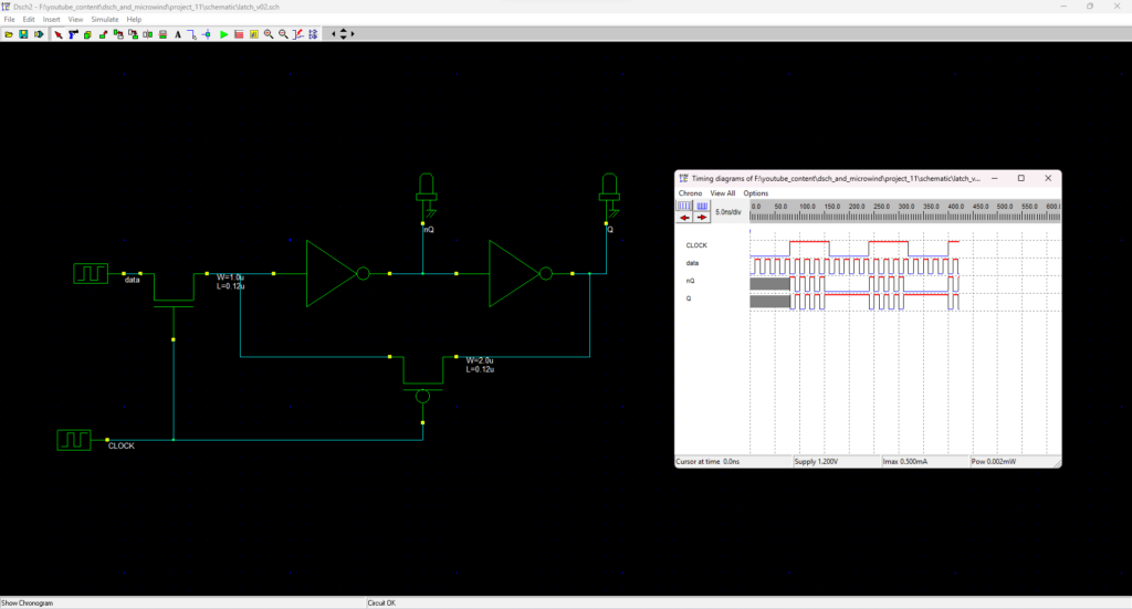
- Launch DSCH tool and open the symbol library.
- Drag and drop two inverters, one P moss transistor, and one N moss transistor onto the workspace.
- Connect the P moss transistor’s source to the higher voltage and its drain to the output and feedback to the inverters.
- Connect the N moss transistor’s drain to the input and its source to the inverters.
- Utilize the ‘Add Line’ option to complete the circuit connections and rename components: outputs as Q and nQ, input to N moss as data, and input to N moss gate as enable.
- Set the on and off times for the enable and data signals, ensuring they are not multiples of each other.
- Simulate the circuit by clicking ‘Simulate’, observe the timing diagram, and stop the simulation to analyze.
- Save the schematic as ‘latch_v01.sch’ and generate the Verilog file by selecting ‘Make Verilog File’. Change the file extension from .TXT to .V.
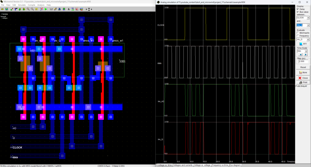
- Open Microwind, select the 0.35 micrometer foundry under the file tab, and compile the Verilog file using the ‘compile Verilog’ option.
- Complete the layout by arranging metal layers and connections, add a VDD connection to the N-well region.
- Run the layout simulation to verify output behavior with varying enable signals and observe frequency and power consumption by using the respective simulation tools.
- Save the final layout as ‘latch_v01.msk’ for future reference.
- Ensure all settings and simulations are accurately documented and adjusted as necessary for complete verification of the latch design.
Results:
After following the steps correctly, the simulation in Microwind show the expected behavior for latch, aligning with the input and output relations defined in the theory section.
Conclusion:
The experiment successfully demonstrates the practical application of schematic to layout conversion for complex designs using DSCH and Microwind.
Viva-Voce Questions:
Certainly! Below are 20 viva voce questions designed for a practical related to the CMOS schematic of a latch using the DSCH tool, generating Verilog netlist, and converting this into layout in Microwind, within a VLSI CMOS design lab context.
Questions Related to CMOS Latch Schematic Using DSCH Tool
Q1: What is a latch in digital electronics?
- A latch is a basic memory device that can hold one bit of data and has two stable states. It captures the input data when a control signal (like a clock) is in a particular state.
Q2: Describe the role of a pass transistor in a latch design.
- A pass transistor controls the flow of data into the latch circuit. It allows or blocks data based on the gate signal, typically connected to a control or clock signal.
Q3: What is the purpose of using inverters in a latch circuit designed in DSCH?
- Inverters are used to maintain the logic levels and create necessary feedback loops in the latch design, ensuring that the latch retains the last input state when the control signal is deactivated.
Q4: How do you simulate a latch in the DSCH tool?
- To simulate a latch in DSCH, you set up the circuit with the required components, apply the input and clock signals, and then use the simulate button to observe the behavior of the latch over time.
Q5: What does converting a DSCH schematic to a Verilog netlist involve?
- Converting a DSCH schematic to a Verilog netlist involves generating a textual representation of the circuit which describes the logic functions and connectivity between components in Verilog code.
Q6: Explain the significance of Verilog in VLSI design.
- Verilog is a hardware description language used in VLSI design to model electronic systems at various levels of abstraction, enabling simulation, testing, and hardware implementation.
Q7: Why is it important to set non-multiple on and off times for the enable and data signals in latch simulation?
- Setting non-multiple times helps in testing the latch under various input conditions, ensuring robustness and verifying that the latch can handle asynchronous signal changes effectively.
Q8: What are the critical aspects to verify in a timing diagram of a latch?
- Critical aspects include checking that the latch holds the output stable when the enable signal is low and passes the input correctly when the enable signal is high.
Q9: How do you ensure a latch design is optimized for area in Microwind?
- In Microwind, area optimization can be achieved by minimizing the number of transistors and optimizing the layout to reduce space and interconnect lengths, often using automated tools provided within Microwind.
Q10: What steps are involved in verifying the functionality of a latch layout in Microwind?
- Verification involves running simulations to ensure the layout performs as expected, checking connectivity, observing the output against various inputs, and ensuring no logical or layout errors exist.
Additional Questions Related to Verilog Conversion and Microwind Layout
Q11: What is the purpose of renaming components in the DSCH schematic?
- Renaming components helps in identifying them easily in the schematic and Verilog code, particularly useful during debugging and simulation.
Q12: How do you handle power connections in a CMOS latch layout in Microwind?
- Power connections in Microwind are handled by ensuring that all power-using components are correctly connected to the VDD and ground, typically using metal layers for stable power distribution.
Q13: Describe the process of compiling a Verilog file in Microwind.
- Compiling a Verilog file in Microwind involves loading the Verilog code into the tool, setting the appropriate technology parameters, and then generating the physical layout from the described logic.
Q14: What are the advantages of using DSCH and Microwind for designing a CMOS latch?
- DSCH and Microwind offer an integrated environment for schematic capture, simulation, Verilog generation, and layout, allowing for rapid prototyping and verification of VLSI designs.
Q15: How does the frequency versus time simulation help in analyzing a latch in Microwind?
- This simulation helps in determining the operating frequency range of the latch, ensuring that it can perform adequately under different clock frequencies.
Q16: Explain the role of FFT in latch design verification in Microwind.
- FFT (Fast Fourier Transform) analysis in latch design helps identify frequency components of the output signal, useful in analyzing signal integrity and the impact of high-frequency components.
Q17: What is the significance of the reset function in Microwind simulations?
- The reset function is crucial for clearing any previous states of the simulation, ensuring that each new simulation run starts from a known good state without residual effects.
Q18: How do you verify that a latch maintains its state correctly in Microwind?
- Verification is done by observing the latch’s output in response to changes in the enable signal and checking if it correctly maintains the state when the enable is low and changes state appropriately when high.
Q19: What does changing the Y parameter values in Microwind simulation achieve?
- Adjusting the Y parameter values allows for better visualization and analysis of specific signal characteristics, such as amplitude variations, during simulation.
Q20: Why is it important to save the layout as ‘latch_v01.msk in Microwind?
- Saving the layout with a specific version name allows for proper documentation and version control, especially useful in iterative design processes and future references.
FAQ
Here are 10 FAQ questions with short answers for a practical based on creating a CMOS schematic of a latch using the DSCH tool of Microwind, generating a Verilog netlist, and converting this Verilog to a layout before simulation.
FAQ on CMOS Schematic and Simulation of Latch Using DSCH and Microwind
Q1: What is the purpose of using NMOS and PMOS transistors in a latch circuit?
- NMOS and PMOS transistors are used in a latch to control data flow based on the enable signal, with NMOS typically passing signals when the gate is high, and PMOS when the gate is low, providing a stable output state in the latch.
Q2: How do I determine which terminal to connect to the input and output in NMOS and PMOS transistors in DSCH?
- For NMOS, connect the input to the drain terminal and link the source to the input of the inverters. For PMOS, connect the higher voltage to the source and the other terminal (drain) to the output as feedback to the inverters.
Q3: Why is the correct connection of NMOS and PMOS transistors crucial in generating Verilog code from DSCH?
- Correct connections ensure that the generated Verilog code accurately represents the intended logic and behavior of the circuit, facilitating proper simulation and layout generation in subsequent stages.
Q4: What are the device properties displayed in DSCH, and why are they important?
- Device properties in DSCH include parameters like channel width, length, and threshold voltage, crucial for defining the electrical characteristics of the transistors, impacting performance such as speed and power consumption.
Q5: How does current flow in NMOS and PMOS devices affect the design of a latch?
- Current flow direction in NMOS (drain to source) and PMOS (source to drain) determines how each transistor behaves under different gate voltages, affecting how they should be connected in a circuit to correctly implement the latch logic.
Q6: What happens if the NMOS and PMOS transistors are incorrectly connected in the DSCH schematic?
- Incorrect connections can lead to faulty logic behavior, where the latch may not maintain its state correctly or may behave unpredictably, leading to errors in the Verilog netlist and the final simulation results.
Q7: Can I modify the properties of NMOS and PMOS transistors in DSCH? If yes, how does it affect the circuit?
- Yes, properties such as the width and length of the transistor gates can be modified in DSCH. Changing these properties can affect the drive strength, speed, and power consumption of the circuit.
Q8: How do I ensure my Verilog netlist correctly represents the schematic designed in DSCH?
- Verify that all connections and properties in the schematic match your design intent, use simulation features in DSCH to test the circuit’s logic before generating the Verilog netlist, and review the generated code for accuracy.
Q9: What should I check in the timing diagram after simulating the latch in DSCH?
- Check that when the enable signal is high, the input data is correctly passed to the output, and when low, the output maintains the previous state, indicating the latch is functioning correctly.
Q10: How do I transition from a Verilog netlist in DSCH to a layout in Microwind?
- After generating the Verilog netlist, use the layout generation features in Microwind to import the Verilog file. Microwind will then compile the netlist to create a physical layout that can be further simulated and optimized for fabrication.
Internal Links:
- JNTUH VLSI Lab Experiments – Explore a series of lab experiments for understanding VLSI design concepts using Xilinx Vivado.
CMOS VLSI LAB CYCLE 01:
Lab Reports and Related YouTube Videos:
- Lab 01: Logic Gates
- Lab 02: Encoder and Decoder
- Lab 03: Multiplexer, Demultiplexer
- Lab 04: Binary to Gray Converter
- Lab 05: Comparator Circuit
- Lab 06: Adder Circuit
CMOS VLSI LAB CYCLE 02:
Lab Reports and Related YouTube Video:
- Lab 01 Part-2: Basic Logic Gates Layout
- Lab 02 Part-2: Basic Logic Gates Layout
- Lab 03 Part-2: NOR and NAND gate design using Microwind
- Lab 04 Part-2: XOR gate and 2:1 Multiplexer design using Microwind