CMOS VLSI Lab using Xilinx Vivado
In the vast and evolving field of electronics and communication engineering, practical skills in digital design hold immense value. One such critical skill is the ability to simulate logic gates using sophisticated software like Xilinx Vivado. This blog post offers a step-by-step guide tailored not just for students following the JNTUH syllabus, specifically the CMOS VLSI DESIGN LABORATORY for B.Tech III Year II Semester, but also for enthusiasts and professionals seeking to deepen their understanding of digital logic design.
Lab report
AIM:
To design and simulate all basic logic gates (AND, OR, NOT, NAND, NOR, XOR, XNOR) using CMOS technology in Xilinx Vivado environment.
Apparatus / Software required:
- Computer System: Adequate specifications to run Xilinx Vivado.
- Software: Xilinx Vivado Design Suite.
Theory:
Logic gates are the fundamental building blocks of any digital system. Each gate has a unique truth table representing its functionality. In CMOS technology, these gates are realized using a combination of PMOS and NMOS transistors. The list below outlines the core concepts:
| A (Input) | B (Input) | AND | OR | NOT A | NAND | NOR | XOR | XNOR |
|---|---|---|---|---|---|---|---|---|
| 0 | 0 | 0 | 0 | 1 | 1 | 1 | 0 | 1 |
| 0 | 1 | 0 | 1 | 1 | 1 | 0 | 1 | 0 |
| 1 | 0 | 0 | 1 | 0 | 1 | 0 | 1 | 0 |
| 1 | 1 | 1 | 1 | 0 | 0 | 0 | 0 | 1 |
- AND Gate: Outputs high (1) only when both A and B are high (1).
- OR Gate: Outputs high (1) if at least one input is high (1).
- NOT Gate (Inverter): Outputs the inverse of input A; here, the table shows NOT A.
- NAND Gate: Outputs low (0) only when both A and B are high (1).
- NOR Gate: Outputs high (1) only when both A and B are low (0).
- XOR Gate: Outputs high (1) when A and B are different.
- XNOR Gate: Outputs high (1) when A and B are the same.
Procedure:
- Launch Xilinx Vivado:
- Start by opening the Xilinx Vivado Design Suite on your computer.
- Create a New Project:
- Navigate to File > New Project. Follow the wizard to set up your project for logic gate simulation.
- Design Entry:
- Choose “Verilog” as the target language and create a new Verilog file named
logic_gates.vfor your gate designs.
- Choose “Verilog” as the target language and create a new Verilog file named
- Implement Logic Gates:
- Write the Verilog code to implement each logic gate. Ensure to include modules for AND, OR, NOT, NAND, NOR, XOR, and XNOR gates.
- Create a Testbench:
- Develop a testbench
logic_gates_tb.vto verify the functionality of your logic gates. The testbench should apply various input combinations and monitor the output for each gate.
- Develop a testbench
- Run Simulation:
- Compile your design and testbench, then run the simulation. Analyze the waveform to verify the functionality of each logic gate.
- Analyze Results:
- Check the output waveforms against the expected truth tables for each logic gate.
Code:
RTL File :logic_gates.v
// logic_gates.v
// This Verilog file realizes all basic logic gates: AND, OR, NOT, NAND, NOR, XOR, and XNOR.

module logic_gates (
    input wire a,
    input wire b,
    output wire and_gate,
    output wire or_gate,
    output wire not_gate_a,
    output wire nand_gate,
    output wire nor_gate,
    output wire xor_gate,
    output wire xnor_gate
);

// Logic gate implementations
assign and_gate = a & b;
assign or_gate = a | b;
assign not_gate_a = ~a;
assign nand_gate = ~(a & b);
assign nor_gate = ~(a | b);
assign xor_gate = a ^ b;
assign xnor_gate = ~(a ^ b);

endmodule
Testbench file: logic_gates_tb.v
// logic_gates_tb.v
// This is a testbench for simulating all basic logic gates realized in logic_gates.v

`timescale 1ns / 1ps

module logic_gates_tb;

// Inputs
reg a;
reg b;

// Outputs
wire and_gate;
wire or_gate;
wire not_gate_a;
wire nand_gate;
wire nor_gate;
wire xor_gate;
wire xnor_gate;

// Instantiate the Unit Under Test (UUT)
logic_gates uut (
    .a(a),
    .b(b),
    .and_gate(and_gate),
    .or_gate(or_gate),
    .not_gate_a(not_gate_a),
    .nand_gate(nand_gate),
    .nor_gate(nor_gate),
    .xor_gate(xor_gate),
    .xnor_gate(xnor_gate)
);

initial begin
    // Initialize Inputs
    a = 0; b = 0;

    // Wait 100 ns for global reset to finish
    #10;

    // Add stimulus here
    a = 0; b = 1; #10;
    a = 1; b = 0; #10;
    a = 1; b = 1; #10;
end

endmodule
Expected Waveform:
- The waveform will display the input and output signals for each logic gate over time. It should match the expected behavior as defined by the truth tables.
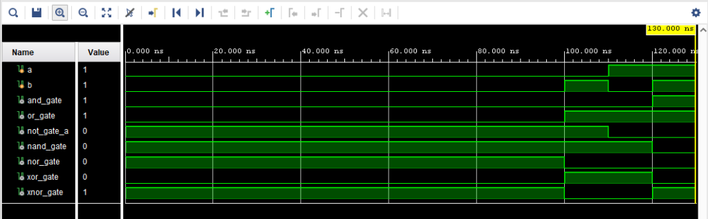
Result:
Upon successful simulation, all logic gates will exhibit outputs in accordance with their respective truth tables, demonstrating the correct realization of logic gates in a CMOS VLSI design environment using Xilinx Vivado.
Conclusion:
This experiment emphasizes the significance of understanding and implementing basic logic gates in the realm of digital design and VLSI. Through the hands-on experience of simulating these gates in Xilinx Vivado, students and researchers gain valuable insights into the intricacies of digital logic and CMOS technology, laying a solid foundation for more complex designs.
Understanding the Basics
Before diving into the technical steps, let’s ensure we have a solid foundation. Logic gates are the building blocks of digital circuits, performing basic logical functions that are fundamental to digital computing. Xilinx Vivado, a state-of-the-art design suite, provides an integrated development environment for designing and simulating logic gates among other advanced digital design tasks.
Preparing Your Workspace
- Creating a Structured Environment: The importance of organizing your files cannot be overstated. We recommend creating a folder named
vivado_simulationand within it, three subfolders:rtl,tb, andvivado project. This structure will keep your project files neatly organized and easily accessible. - Downloading Necessary Files: To get started, you will need Verilog code files for the logic gates and a testbench to simulate them. These files can be typically found in the resources section provided by your instructor or the specific lab manual for the CMOS VLSI DESIGN LABORATORY.
Step-by-Step Guide to Creating and Simulating a Vivado Project
- Launch Vivado and Create a New Project: Begin by opening Xilinx Vivado and selecting the option to create a new project. Make sure to navigate to your
vivado_simulationfolder and create the project within thevivado projectsubfolder. - Setting Up the Project: Choose ‘RTL Project’ and proceed without specifying sources at this time. This approach allows you to add your source files (the Verilog code for the logic gates) later in the process.
- Adding Source Files: Learn how to add your RTL (Register Transfer Level) design source (
logic_gates.v) and your testbench (logic_gates_tb.v) to the project. These steps are crucial for preparing your project for simulation. - Running the Simulation: With your source files added, the next step is to run a behavioral simulation. This process involves compiling your Verilog code and executing the simulation to observe the behavior of your logic gates under various input conditions.
Analyzing Simulation Results
- Interpreting Waveforms: Understanding how to read and interpret the waveforms generated by the simulation is key to verifying the functionality of your logic gates. This section will provide insights into analyzing these waveforms to ensure your design meets the desired specifications.
- Troubleshooting Common Issues: It’s not uncommon to encounter issues during simulation. We’ll cover some basic troubleshooting steps to help you resolve common problems, such as missing signals or unexpected logic levels.
Beyond the Basics
- Optimizing Your Design: Once you’re comfortable with basic simulations, you might want to explore more advanced topics, such as optimizing your Verilog code for better performance or lower power consumption.
- Real-World Applications: Understanding how logic gates can be combined to create more complex digital circuits is crucial. We’ll discuss how the skills you’ve developed can be applied to real-world digital design projects.
Conclusion
This guide aims to demystify the process of simulating logic gates using Xilinx Vivado, making it accessible to students and hobbyists alike. Whether you’re following the JNTUH syllabus or exploring digital design on your own, this tutorial provides a solid foundation for advancing your skills in the fascinating world of digital electronics.
Encouraging Further Exploration
- Resources for Advanced Learning: For those eager to dive deeper, we’ll recommend additional resources, including textbooks, online courses, and community forums, where you can further explore the subjects of digital design and Verilog coding.
- Community and Support: The journey of learning digital design is both challenging and rewarding. Joining communities and seeking support from fellow learners and professionals can provide valuable insights and encouragement as you progress.
By following this guide, you’re well on your way to mastering the simulation of logic gates in Vivado, a skill that will serve you well in your studies, hobby projects, or
professional endeavors in electronics and digital design. Happy simulating!
Frequently Asked Questions (FAQ)
- Can this guide be used by those not following the JNTUH syllabus?
- Absolutely! While this guide is tailored to the requirements of the CMOS VLSI DESIGN LABORATORY course in the JNTUH syllabus, the skills and techniques are universally applicable in the field of digital design.
- What if I encounter errors during simulation?
- Errors are a normal part of the learning process. This guide includes a troubleshooting section to help you identify and resolve common issues. Always start by checking your Verilog code for syntax errors and ensuring your simulation environment is correctly set up.