Welcome to our comprehensive guide on the simulation and analysis of a CMOS inverter, tailored for students and professionals engaged in semiconductor design and VLSI technology. This blog serves as an educational resource for the CMOS VLSI DESIGN LABORATORY, specifically designed for B.Tech. III Year II Semester students under the JNTUH curriculum. The CMOS inverter, a pivotal component in digital electronics, provides the necessary foundation for understanding the operational principles and design strategies of more complex integrated circuits.
In this guide, we will delve into the intricacies of the CMOS inverter’s design process, starting from layout generation to the critical analyses required to ensure robust and efficient performance. Our aim is to equip you with a solid understanding of layout design, physical verification, placement and routing, static timing analysis, IR drop analysis, and crosstalk analysis. By the end of this tutorial, you will be able to simulate these aspects using MicroWind an important electronic design automation (EDA) tool.
This blog will not only provide step-by-step instructions on how to simulate a CMOS inverter but will also cover theoretical concepts, practical results, and common troubleshooting practices. Whether you are a student preparing for lab exams or a budding engineer designing your next project, this guide will be your go-to reference for CMOS inverter design and analysis.
Lab Report
AIM: Layout Design and Simulation of CMOS Inverter
Apparatus / Software required:
- Windows Machine with Microwind Software Installed
Theory:
Theory: CMOS Inverter Design and Operation
The CMOS inverter is the most fundamental logic gate in digital circuit design, forming the backbone of modern VLSI systems. This simple yet powerful device consists of a pair of MOSFETs (Metal-Oxide-Semiconductor Field-Effect Transistors): one p-type (PMOS) and one n-type (NMOS). The PMOS and NMOS are configured in a complementary manner such that the output voltage is the logical inverse of the input voltage.
Operational Principle:
- PMOS: This transistor is on (conducting) when the gate voltage is low relative to its source, which is typically connected to the positive supply voltage (Vdd).
- NMOS: This transistor conducts when the gate voltage is high relative to its source, which is typically grounded.
In a CMOS inverter:
- When the input (VIN) is high (logic ‘1’), the NMOS is on, allowing current to flow from the output (VOUT) to ground, pulling VOUT low (logic ‘0’).
- Conversely, when VIN is low (logic ‘0’), the PMOS is on, connecting VOUT to Vdd, thus making VOUT high (logic ‘1’).
The complementary action of the PMOS and NMOS ensures that there is no direct path from Vdd to ground at any time, significantly reducing power consumption when the state is stable.
Layout Considerations:
The layout of a CMOS inverter involves placing the PMOS and NMOS transistors in such a way that they occupy minimal area while still adhering to design rules for spacing and alignment. Key layout considerations include:
- Well Taps: Ensuring that p-wells and n-wells are properly connected to their respective supply voltages to prevent latch-up.
- Interconnects: Minimizing the length and resistance of interconnects to reduce parasitic capacitance and enhance speed.
- Symmetry: Designing a symmetrical layout to ensure uniform electrical characteristics and simplify the manufacturing process.
Input and Output Relationship:
The table below illustrates the relationship between the input and output of a CMOS inverter, which is a straightforward inverse relationship:
| Input (VIN) | Output (VOUT) |
|---|---|
| High (Logic ‘1’) | Low (Logic ‘0’) |
| Low (Logic ‘0’) | High (Logic ‘1’) |
Understanding the fundamental operation and layout considerations of the CMOS inverter not only aids in grasping this specific circuit’s function but also sets a foundation for more complex logic gate designs in integrated circuits. This knowledge is crucial for anyone aiming to excel in the field of VLSI design.
Procedure:
- Start MicroWind: Double-click on “Microwind31.exe – Shortcut” to open the software.
- Open the Layout Generator: Navigate to the “Layout Generator” from the main window.
- Set Parameters: In the “Layout Generator”, select “in lambda” and adjust the MOS parameters as required.
- Design Layout: Drag and drop MOS components from the “Palette” into the layout area, adjusting their size and connections according to the inverter design.
- Compile Design: Click on “Compile” to generate the layout and check for any initial errors.
- Assign Inputs and Outputs: Use the “Palette” to assign inputs and output labels, e.g., A_in for input A, and set their clock frequencies.
- Simulation Setup: Configure the simulation parameters, including input frequencies and output waveforms.
- Run Simulation: Click on “Run Simulation” to view the operational behavior of the CMOS inverter.
- Adjust Visual Settings: If necessary, change the background color via “Colors” in the “File” menu to enhance waveform visibility.
- Analyze Results: Review the output waveforms and parameters such as voltage levels and power consumption.
- Save and Document: Capture screenshots of important results using the snipping tool, and save the project using “Save As” from the “File” menu.
- Reset and Re-test: Perform additional tests by resetting the simulation and changing input conditions as needed.
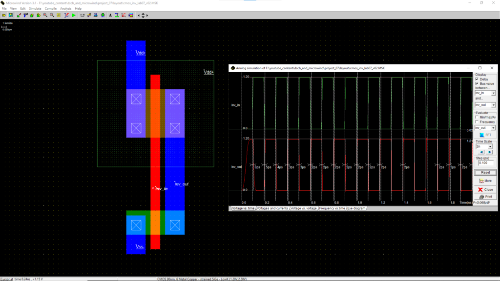
Results:
After following the steps correctly, the simulation in Microwind show the expected behavior for CMOS Inverter, aligning with the input and output relations defined in the theory section.
Conclusion:
In conclusion, the CMOS inverter design and simulation using Microwind effectively demonstrates the fundamental principles and practical implementation techniques of CMOS inverters.
Viva-Voce Questions:
Here are 10 Viva Voce questions for a practical based on the title “CMOS Inverter Design and Simulation using Microwind” as part of a VLSI CMOS design lab:
Q1: What is the purpose of a CMOS inverter in VLSI design?
- The purpose of a CMOS inverter in VLSI design is to provide a basic switching operation where it inverts the input signal; a logical ‘1’ becomes ‘0’ and vice versa, serving as a fundamental building block in digital circuits.
Q2: Can you describe the basic structure of a CMOS inverter?
- A basic CMOS inverter consists of two transistors: an n-channel MOSFET and a p-channel MOSFET. The n-channel MOSFET is connected to ground, and the p-channel MOSFET is connected to the supply voltage. The input signal controls both transistors, creating an inverted output.
Q3: How does the CMOS inverter switch states?
- The CMOS inverter switches states based on the input signal. When the input is high (logic 1), the p-channel MOSFET turns off and the n-channel MOSFET turns on, driving the output to low (logic 0). Conversely, when the input is low, the p-channel MOSFET turns on and the n-channel MOSFET turns off, driving the output high.
Q4: What are the advantages of using CMOS technology for inverters?
- CMOS technology offers significant advantages for inverters, including lower power consumption, higher noise immunity, and better scaling properties. It also produces less heat and supports a high density of logic functions on a chip.
Q5: What is propagation delay in a CMOS inverter?
- Propagation delay in a CMOS inverter is the time it takes for the input change to affect the output. This delay occurs due to the time required to charge or discharge the load capacitance through the MOSFETs.
Q6: Why is the W/L ratio important in the design of CMOS inverters?
- The width-to-length (W/L) ratio of the MOSFETs in a CMOS inverter affects the current carrying capability of the transistors, which in turn impacts the inverter’s switching speed and drive strength. Proper sizing is critical for optimizing performance and minimizing power consumption.
Q7: What happens during the transient response of a CMOS inverter?
- During the transient response, the output voltage of the CMOS inverter transitions between high and low states. This period is characterized by charging and discharging of load capacitors, and the speed of this response is a critical performance metric.
Q8: How does temperature affect the performance of a CMOS inverter?
- Temperature variations can affect the performance of a CMOS inverter by changing the mobility of the carriers in the MOSFET channels, which affects the current drive capabilities and thus the speed and stability of the inverter.
Q9: What is the significance of the threshold voltage in a CMOS inverter?
- The threshold voltage is the minimum gate-to-source voltage difference needed to turn the MOSFET from off to on. It is crucial for determining the switching point of the inverter and affects the noise margin and power consumption of the circuit.
Q10: How do load capacitance and supply voltage affect the operation of a CMOS inverter?
- Load capacitance affects how quickly the output can transition between states, impacting the propagation delay. Supply voltage affects the overall speed and power efficiency of the inverter; higher voltages typically decrease the delay but increase power consumption.
CMOS Inverter Layout Design – Fundamental concepts
“To explain why the width of the PMOS transistor is often designed to be approximately twice that of the NMOS transistor in a CMOS inverter, it’s crucial to understand how the transistor’s dimensions affect the propagation delays during the low-to-high (tpLH) and high-to-low (tpHL) transitions.
Propagation Delay Equations
The propagation delays tpHL and tpLH for a CMOS inverter are given by:
tpHL = CL VDD/IDn
tpLH = CL VDD/IDp
Where:
- CL is the load capacitance.
- VDD is the supply voltage.
- IDn and IDp are the drain currents of the NMOS and PMOS, respectively, under saturation conditions.
Current Equation
The drain current ID in saturation for both NMOS and PMOS can be expressed as:
ID = 1/2 μ Cox (W/L) (VGS – VT)2
Given that the electron mobility (μn) is typically higher than hole mobility (μp), it follows that:
IDn = 1/2 μn Cox (Wn/Ln) (VGS – VTn)2
IDp = 1/2 μp Cox (Wp/Lp) (VSG – VTp)2
Balancing Propagation Delays
To achieve equal rise and fall times, we aim to equalize tpHL and tpLH. Setting the two equations equal gives:
CL VDD/IDn = CL VDD/IDp
This simplifies to:
IDn = IDp
Substituting the drain current expressions, we have:
1/2 μn Cox (Wn/Ln) (VGS – VTn)2 = 1/2 μp Cox (Wp/Lp) (VSG – VTp)2
For simplification, assuming the length L and threshold voltages VT are equal for both transistors and the voltage terms are constant across transitions, the equation reduces to:
μn Wn = μp Wp
Determining Width Ratio
Now solving for Wp/Wn:
Wp/Wn = μn/μp
Given typical values where μn (electron mobility) is roughly two to three times μp (hole mobility), this leads to:
Wp/Wn ≈ 2 to 3
Conclusion
Thus, to compensate for the lower hole mobility in PMOS relative to the electron mobility in NMOS and to equalize the driving currents necessary for similar propagation delays, the width Wp of the PMOS transistor is typically made two to three times larger than the width Wn of the NMOS transistor. This is why, in many designs, you might see PMOS transistors with approximately twice the width of their NMOS counterparts. This design strategy helps achieve balanced
switching characteristics and equal rise and fall times in CMOS inverters.”
FAQ
Here are 10 FAQ questions about the blog for the experiment “CMOS Inverter Design and Simulation using Microwind,” focusing on the tool Microwind and VLSI layout design in general:
Q1: What is Microwind and how is it used in VLSI design?
- Microwind is a specialized software tool used for designing and simulating microelectronic systems at the circuit and layout level. It is widely used in VLSI design for educational and research purposes, enabling users to create and test designs before fabrication.
Q2: Can I simulate complex VLSI circuits using Microwind?
- Yes, Microwind supports the simulation of complex VLSI circuits. It includes various tools for digital, analog, and mixed-signal designs, allowing users to simulate the behavior and performance of their circuits under different conditions.
Q3: What file formats does Microwind support for exporting and importing designs?
- Microwind allows importing from and exporting to various standard file formats used in VLSI design, including GDSII for mask design, CIF for integrated circuit layouts, and more, facilitating easy integration with other industry-standard tools.
Q4: How accurate are the simulations in Microwind compared to real-world results?
- Simulations in Microwind are highly accurate, closely mirroring real-world results. The tool includes accurate models for transistor behavior, interconnect, and layout parasitics, which help predict the performance of the designed circuits effectively.
Q5: What are the system requirements to run Microwind effectively?
- Microwind requires a Windows or Linux operating system, with recommended specifications including a modern processor, at least 4GB of RAM, and sufficient hard disk space for complex projects. A good graphics card is also recommended for rendering detailed layouts.
Q6: How can I optimize my VLSI design for low power consumption using Microwind?
- To optimize VLSI designs for low power consumption in Microwind, focus on minimizing leakage currents and dynamic power. Techniques include scaling down supply voltages, optimizing the threshold voltage of transistors, and using power gating methods.
Q7: Does Microwind provide any tutorials for beginners in VLSI design?
- Yes, Microwind includes a variety of tutorials and documentation aimed at beginners. These resources cover fundamental concepts of VLSI design and provide step-by-step instructions on using the software for various design tasks.
Q8: Can Microwind simulate the thermal effects in VLSI circuits?
- Microwind is capable of simulating the thermal effects in VLSI circuits, which is crucial for understanding the impact of heat on circuit performance, reliability, and longevity.
Q9: What kind of support does Microwind offer for educational institutions?
- Microwind offers extensive support for educational institutions, including academic licensing, specialized training materials, and access to a community of users and experts who can provide guidance and share best practices.
Q10: How do I handle layout verification in Microwind to ensure my design meets all specifications?
- Layout verification in Microwind can be handled through its built-in DRC (Design Rule Check) and LVS (Layout Versus Schematic) tools, which automatically check for common errors and ensure that the layout correctly matches the schematic design and meets all fabrication rules.
Internal Links:
- JNTUH VLSI Lab Experiments – Explore a series of lab experiments for understanding VLSI design concepts using Xilinx Vivado.
CMOS VLSI LAB CYCLE 01:
Lab Reports and Related YouTube Videos:
- Lab 01: Logic Gates
- Lab 02: Encoder and Decoder
- Lab 03: Multiplexer, Demultiplexer
- Lab 04: Binary to Gray Converter
- Lab 05: Comparator Circuit
CMOS VLSI LAB CYCLE 02:
Lab Reports and Related YouTube Video:
- Lab 01 Part-2: Basic Logic Gates Layout
These resources provide a comprehensive overview and practical insights into various aspects of CMOS VLSI design, offering valuable information for students and enthusiasts interested in exploring the field of VLSI design using Xilinx Vivado and Microwind.