Welcome to our educational blog focused on a key component of the CMOS VLSI Design Laboratory for B.Tech III Year II Semester students at JNTUH. This session, we delve deep into the practical aspects of microelectronic design, specifically through the creation of NOR and NAND gate layouts using the Micro Wind software tool.
Micro Wind is integral to the field of VLSI (Very Large Scale Integration) design, offering robust simulation and layout capabilities that allow students and professionals to create intricate designs at the microchip level. This software is especially critical in understanding the physical layout and electrical behavior of CMOS (Complementary Metal-Oxide-Semiconductor) circuits.
In this blog, we will explore the structured process outlined in the JNTUH curriculum, guiding you through detailed steps to design NOR and NAND gates, which are essential building blocks in digital electronics. These gates play crucial roles in logic circuits, influencing everything from basic computing tasks to complex system operations.
This guide is designed to not only provide a practical approach to VLSI design but also to enhance your learning experience by connecting theoretical concepts with real-world application. Whether you’re a student at JNTUH, an aspiring engineer, or an electronics enthusiast, this article aims to equip you with the skills and knowledge needed to excel in the dynamic field of microelectronics design. Join us as we embark on this detailed exploration of NOR and NAND gate layouts, a cornerstone topic in advanced electronic design.
Lab Report
AIM: Layout Design and Simulation of CMOS NOR/NAND Gates
Apparatus / Software required:
- Windows Machine with Microwind Software Installed
Theory:
Theory: CMOS Inverter Design and Operation
Theory Section: Understanding NOR and NAND Gates
Overview
NOR and NAND gates are fundamental components of digital electronics. These gates process binary inputs (0s and 1s) to produce a specific output, based on the type of gate and the combination of inputs. In simple terms, these gates perform basic logical operations that are integral to the functioning of various digital systems.
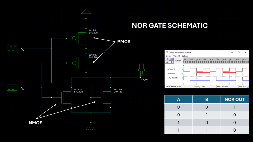
NOR Gate
A NOR gate is a digital logic gate that outputs true or 0 only when all its inputs are false or 0. If any of the inputs are true or 1, the output is false or 0. The NOR gate can be seen as a combination of an OR gate followed by a NOT gate. It is used extensively in digital circuits to implement negations and combinations of logical functions.
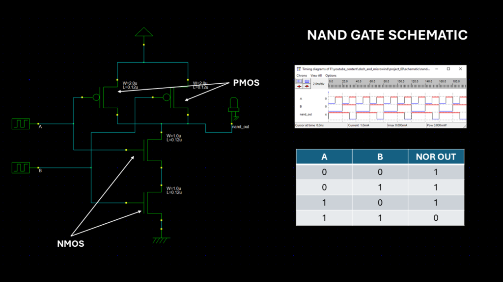
NAND Gate
A NAND gate operates as the inverse of an AND gate. It provides an output of true or 1 unless all its inputs are true or 1, in which case it outputs false or 0. Essentially, a NAND gate delivers an output of 0 only when all inputs are 1. This gate is crucial in digital electronics because it can be used to construct any other logic gate, making it universal in the realm of digital circuits.
Truth Table for NOR and NAND Gates
Combined Truth Table for NOR and NAND Gates
The table below clearly shows the relationship between the inputs and outputs for both NOR and NAND gates:
| Input A | Input B | NOR Output | NAND Output |
|---|---|---|---|
| 0 | 0 | 1 | 1 |
| 0 | 1 | 0 | 1 |
| 1 | 0 | 0 | 1 |
| 1 | 1 | 0 | 0 |
The Importance of Schematic to Layout Conversion in CMOS VLSI Design
In CMOS VLSI design, converting a schematic diagram into a physical layout is a critical step. This conversion is essential because it allows designers to visualize and test how an electronic circuit will behave in the real world. By transforming theoretical schematics into tangible layouts, designers can identify potential issues like parasitic capacitance or layout-induced noise, which might not be apparent in the schematic stage. This process also facilitates the integration of multiple transistors onto a single chip, optimizing space and improving performance.
Advantages:
- Accuracy: Converting schematics to layouts helps in achieving precise control over component placement and routing, reducing errors.
- Efficiency: It allows for the efficient use of silicon space, essential in high-density designs like CPUs and memory chips.
- Verification: Physical layouts can be extensively simulated and tested for electrical integrity, ensuring reliability before fabrication.
Disadvantages:
- Complexity: The process can be complex and time-consuming, requiring specialized tools and skills.
- Cost: High-quality design tools and simulations are expensive, increasing the overall cost of development.
- Rigidity: Once a layout is fabricated, making changes can be costly and cumbersome, often requiring significant rework of the design.
Overall, the schematic to layout conversion is a pivotal process in CMOS VLSI design that bridges the gap between theoretical design and practical application, providing a critical check before moving to the production of electronic components.
Procedure:
- Open the DSCH tool by double-clicking its icon to design a NOR gate schematic.
- From the symbol library, select and place two PMOS devices in series and two NMOS devices in parallel on the schematic window.
- Connect ground, VDD supply, and label clock inputs as ‘A’ and ‘B’.
- Use the ‘add a line’ option to make connections between the PMOS and NMOS devices, assigning inputs A and B respectively.
- Place a LED to represent the output and label it ‘nor_out’.
- Run the simulation to verify the NOR gate operation, checking the timing diagram for accuracy.
- Save the project as ‘nor_basic_lab09.sch’ and generate a Verilog file using the ‘Make Verilog File’ option from the file menu.
- Convert the saved Verilog TXT file to a ‘.v’ file by renaming it.
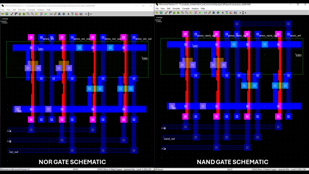
- Open Microwind, compile the Verilog file, ensuring to select the correct library, especially for PMOS devices suitable for 2-micrometer rules.
- Adjust the VDD and VSS connections, assign the clock inputs with their respective frequencies, and label the output node ‘nor_out’.
- Run another simulation in Microwind to confirm the layout’s functionality, observing power and frequency characteristics.
- Save the finalized design as a MSK file for further usage or reference.
- Repeat the same steps to design NAND gate and verify its opearation.
Results:
After following the steps correctly, the simulation in Microwind show the expected behavior for CMOS NOR and NAND gate, aligning with the input and output relations defined in the theory section.
Conclusion:
The experiment successfully demonstrates the practical application of schematic to layout conversion for complex designs using DSCH and Microwind.
Viva-Voce Questions:
Here are 10 viva voce questions along with their short answers related to the practical on creating CMOS schematics of NOR gates using the DSCH tool of Microwind, generating Verilog netlists, converting these to layouts, and running simulations in a VLSI CMOS design lab.
Q1: What is the role of the DSCH tool in the design of a NOR gate?
- The DSCH tool is used for creating and simulating digital schematics of circuits, including NOR gates, allowing for the verification of logic and timing before converting the design into a physical layout.
Q2: Why do you use PMOS and NMOS transistors in a NOR gate design?
- PMOS and NMOS transistors are used in a complementary arrangement in CMOS technology to ensure low power consumption and high noise immunity. In a NOR gate, PMOS transistors are used in series, and NMOS transistors in parallel to achieve the desired logic output.
Q3: What is a Verilog netlist, and how is it generated from DSCH?
- A Verilog netlist is a description of the circuit in Verilog code, representing the connectivity of transistors as used in the schematic. It is generated from DSCH by exporting the schematic design into Verilog format, capturing the logical structure of the circuit.
Q4: What is the significance of converting a Verilog netlist to a layout in Microwind?
- Converting a Verilog netlist to a layout in Microwind is crucial for visualizing the physical placement of components and interconnections on silicon, which aids in understanding the fabrication process and enables further simulation and testing of the physical characteristics of the circuit.
Q5: How do you validate the functionality of a NOR gate in DSCH?
- The functionality of a NOR gate in DSCH is validated by running simulations to observe the output for various combinations of input values, ensuring that the output adheres to the truth table of a NOR gate.
Q6: Describe the process of connecting PMOS and NMOS devices in the schematic for a NOR gate.
- In the NOR gate schematic, two PMOS devices are connected in series at the source to VDD and their drains to the output, while two NMOS devices are connected in parallel with their sources to ground and drains also connected to the output.
Q7: What challenges might you encounter when converting a Verilog netlist to a layout?
- Challenges may include handling the complexities of layout rules, ensuring the accuracy of the connections as per the netlist, managing the physical space efficiently, and resolving any errors or mismatches between the schematic and the layout.
Q8: What does the simulation in Microwind show after converting the Verilog to layout?
- The simulation in Microwind after converting Verilog to layout shows the electrical behavior of the NOR gate, including the voltage and current characteristics at different nodes, and verifies the functional correctness of the layout.
Q9: How does changing the input frequencies affect the NOR gate simulation in Microwind?
- Changing the input frequencies affects the switching characteristics and timing of the NOR gate, potentially influencing the gate’s response time and overall performance in high-frequency applications.
Q10: What is the purpose of saving the final design as an MSK file in Microwind?
- Saving the final design as an MSK file in Microwind is essential for preserving the completed layout, which can be used for further analysis, modification, or direct fabrication, serving as a permanent record of the designed circuit.
FAQ
Here are 10 FAQ questions focused on schematic to layout conversion using EDA tools in general, relevant to the practical on creating CMOS schematics of NOR gates and further processing using DSCH and Microwind:
Q1: What is schematic to layout conversion in VLSI design?
- Schematic to layout conversion involves translating a circuit’s schematic diagram, which is a symbolic representation, into a physical layout used for fabrication. This layout details the exact placement of transistors and interconnections on a silicon chip.
Q2: Why is it important to use EDA tools for schematic to layout conversion?
- EDA (Electronic Design Automation) tools automate the complex process of converting schematics into precise physical layouts, ensuring accuracy, efficiency, and compliance with fabrication technology rules, which is critical for the successful manufacturing of VLSI chips.
Q3: How do DSCH and Microwind interact during the design process?
- DSCH is used for designing and simulating the schematic diagram of the circuit, while Microwind takes the Verilog netlist generated from DSCH to create and simulate the physical layout, ensuring the design meets specific technological constraints.
Q4: What is a Verilog netlist, and why is it crucial in the conversion process?
- A Verilog netlist is a text format that describes the components and their connections in a digital circuit. It is crucial because it serves as a bridge between the schematic design and the physical layout, allowing the design to be simulated and physically implemented.
Q5: Can layout conversion be performed manually, or is automation necessary?
- While manual layout conversion is possible, it is time-consuming and prone to errors. Automation using EDA tools is necessary for handling complex circuits, ensuring precision, and speeding up the design process to meet modern technological demands.
Q6: What challenges are associated with converting complex schematics to layouts?
- Challenges include managing signal integrity, avoiding physical and electrical interference, optimizing space, adhering to fabrication rules, and ensuring the layout accurately reflects the schematic while maintaining functionality and performance.
Q7: How do changes in the schematic affect the layout in the conversion process?
- Changes in the schematic require corresponding updates in the layout. This can involve adjusting the placement of components, rerouting connections, and potentially redesigning sections of the layout to accommodate the schematic modifications.
Q8: What role does simulation play after converting a schematic to a layout?
- Simulation post-conversion is vital to verify that the layout behaves as expected, testing for functionality, reliability, and compliance with performance specifications. It helps identify and rectify any issues before the chip goes into production.
Q9: How are errors handled during the schematic to layout conversion?
- Errors are typically handled by EDA tools through design rule checks (DRC) and layout versus schematic (LVS) checks, which ensure that the layout adheres to all manufacturing guidelines and accurately represents the schematic design.
Q10: What steps should be taken if the layout does not function as intended after conversion?
- If the layout does not function as intended, it should be analyzed for errors using debugging tools within the EDA software. Adjustments might be necessary in the schematic design, Verilog netlist, or the layout itself, followed by re-simulation to ensure correct functionality.
Internal Links:
- JNTUH VLSI Lab Experiments – Explore a series of lab experiments for understanding VLSI design concepts using Xilinx Vivado.
CMOS VLSI LAB CYCLE 01:
Lab Reports and Related YouTube Videos:
- Lab 01: Logic Gates
- Lab 02: Encoder and Decoder
- Lab 03: Multiplexer, Demultiplexer
- Lab 04: Binary to Gray Converter
- Lab 05: Comparator Circuit
- Lab 06: Adder Circuit
CMOS VLSI LAB CYCLE 02:
Lab Reports and Related YouTube Video:
- Lab 01 Part-2: Basic Logic Gates Layout
- Lab 02 Part-2: Basic Logic Gates Layout
These resources provide a comprehensive overview and practical insights into various aspects of CMOS VLSI design, offering valuable information for students and enthusiasts interested in exploring the field of VLSI design using Xilinx Vivado and Microwind.