Welcome to our latest blog post, where we delve into the fascinating world of digital design using Xilinx Vivado. Today, we’re focusing on a fundamental yet incredibly versatile component of digital electronics: the full adder. This tiny powerhouse plays a crucial role in the arithmetic logic units at the heart of most digital systems, including computers and mobile devices.
In this blog, we will guide you through an experiment designed to not only teach you the workings of a full adder but also introduce you to three different modeling styles in Verilog: Behavioral, Dataflow, and Structural. Each style offers unique insights and benefits, and understanding them is key to becoming proficient in digital circuit design.
We’ll start by defining what a full adder is and the role it plays in complex digital systems. Then, we’ll explore how to design a full adder using each of the three Verilog modeling styles. The culmination of our experiment will be a practical session in Xilinx Vivado, where we will simulate a full adder.
Whether you’re a student, a budding engineer, or just a technology enthusiast, this experiment will equip you with the skills and knowledge to embark on your own digital design projects. So, let’s get started and dive into the exciting world of digital electronics with Xilinx Vivado!
Lab Report
AIM: Design of Full adder using 3 modeling styles
Apparatus / Software required:
- Xilinx Vivado Design Suite
- Windows Machine
- Notepad or any text editor
Theory:
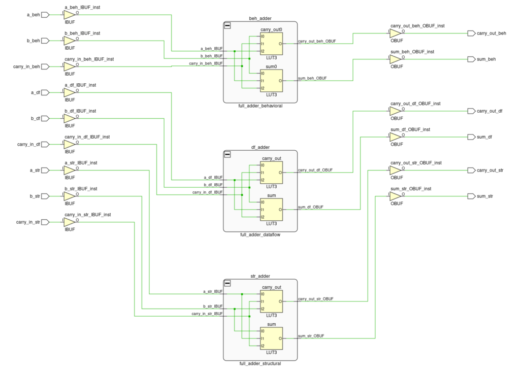
A full adder is a digital circuit that computes the sum of three binary bits, producing a sum and a carry output. It is essential in creating more complex arithmetic circuits like adders and multipliers. In Verilog, there are three primary modeling styles: Behavioral, Dataflow, and Structural. These styles not only offer different levels of abstraction but also help in understanding the flexibility and power of Verilog for designing digital systems. Below, we explore the design of a full adder using these three styles, and simulating it using Xilinx Vivado.
Behavioral Modeling uses high-level programming constructs similar to C or Python, making it straightforward to write and understand. It describes the circuit in terms of how the output relates to the input logically. For a full adder, this can involve using if-else conditions or case statements to determine the sum and carry based on the inputs.
Dataflow Modeling expresses the circuit in terms of data flow between operators. This style uses continuous assignments to describe relationships between inputs and outputs directly. It’s more hardware-oriented than behavioral, as it closely represents how data moves through the circuit.
Structural Modeling describes the circuit as a composition of lower-level components (like gates) and their interconnections. This is the most explicit way of describing a circuit and closely matches the actual hardware.
The table illustrating how inputs relate to the outputs in a full adder:
| Input A | Input B | Carry In | Sum | Carry Out |
|---|---|---|---|---|
| 0 | 0 | 0 | 0 | 0 |
| 0 | 0 | 1 | 1 | 0 |
| 0 | 1 | 0 | 1 | 0 |
| 0 | 1 | 1 | 0 | 1 |
| 1 | 0 | 0 | 1 | 0 |
| 1 | 0 | 1 | 0 | 1 |
| 1 | 1 | 0 | 0 | 1 |
| 1 | 1 | 1 | 1 | 1 |
The full adder serves as a building block in designing more complex systems like the 4-bit comparator, where multiple full adders can be interconnected to compare two 4-bit numbers. The practical experience in simulation will help reinforce the theoretical concepts and demonstrate the practical usage of these modeling styles in real-world applications.
Procedure:
- Open Notepad or any text editor on a Windows machine and write the Verilog code for Full Adder using Behavioral, Dataflow and Structural modeling and corresponding testbench.
- Save the files with a
.vextension, selecting “All Files” as the save type. - Launch Xilinx Vivado from the desktop or start menu.
- Create a new project, naming it appropriately (e.g.,
full_adder_lab06) and choosing the project’s storage location. - Ensure “RTL Project” is selected and specify sources at this time by pointing to the Verilog source code and testbench files you’ve created.
- Select the FPGA board or part targeted for this project using the search function.
- Run Behavioral Simulation to compile the Verilog files and execute the simulation based on your testbench.
- Inspect the waveform viewer to verify that the outputs match the expected results based on your testbench scenarios.
- Proceed with Synthesis and Implementation phases to optimize the design for performance and resource utilization.
- Analyze the simulation results, synthesized schematic, and implementation reports, making necessary adjustments to refine your design.
Code
Full Adder Behavioral Modeling:
// Full adder using behavioral modeling
module full_adder_behavioral(sum, carry_out, a, b, carry_in);
    input a, b, carry_in;
    output reg sum, carry_out;
    always @ (a or b or carry_in) begin
        sum = a ^ b ^ carry_in;
        carry_out = (a & b) | (b & carry_in) | (carry_in & a);
    end
endmodule
Full Adder Dataflow Modeling:
// Full adder using dataflow modeling
module full_adder_dataflow(sum, carry_out, a, b, carry_in);
    input a, b, carry_in;
    output sum, carry_out;
    assign sum = a ^ b ^ carry_in;
    assign carry_out = (a & b) | (b & carry_in) | (carry_in & a);
endmodule
Full Adder Structural Modeling:
// Full adder using structural modeling
module full_adder_structural(sum, carry_out, a, b, carry_in);
    input a, b, carry_in;
    output sum, carry_out;
    wire w1, w2, w3;
    xor (sum, a, b, carry_in);
    and (w1, a, b);
    and (w2, a, carry_in);
    and (w3, b, carry_in);
    or (carry_out, w1, w2, w3);
endmodule
Top-level module integrating all full adder designs:
// Top-level module integrating all full adder designs with separate inputs
module top_full_adder(
    input a_beh, b_beh, carry_in_beh,    // Inputs for the behavioral adder
    input a_df, b_df, carry_in_df,       // Inputs for the dataflow adder
    input a_str, b_str, carry_in_str,    // Inputs for the structural adder
    output sum_beh, carry_out_beh,
    output sum_df, carry_out_df,
    output sum_str, carry_out_str
);

// Instantiating the behavioral adder
full_adder_behavioral beh_adder (
    .sum(sum_beh),
    .carry_out(carry_out_beh),
    .a(a_beh),
    .b(b_beh),
    .carry_in(carry_in_beh)
);

// Instantiating the dataflow adder
full_adder_dataflow df_adder (
    .sum(sum_df),
    .carry_out(carry_out_df),
    .a(a_df),
    .b(b_df),
    .carry_in(carry_in_df)
);

// Instantiating the structural adder
full_adder_structural str_adder (
    .sum(sum_str),
    .carry_out(carry_out_str),
    .a(a_str),
    .b(b_str),
    .carry_in(carry_in_str)
);

endmodule
Testbench for the Top module:
// Testbench for the top_full_adder module
module testbench_to_adder;
    reg a_beh, b_beh, carry_in_beh;
    reg a_df, b_df, carry_in_df;
    reg a_str, b_str, carry_in_str;
    wire sum_beh, carry_out_beh;
    wire sum_df, carry_out_df;
    wire sum_str, carry_out_str;

    // Instantiate the top module
    top_full_adder uut (
        .a_beh(a_beh), .b_beh(b_beh), .carry_in_beh(carry_in_beh),
        .a_df(a_df), .b_df(b_df), .carry_in_df(carry_in_df),
        .a_str(a_str), .b_str(b_str), .carry_in_str(carry_in_str),
        .sum_beh(sum_beh), .carry_out_beh(carry_out_beh),
        .sum_df(sum_df), .carry_out_df(carry_out_df),
        .sum_str(sum_str), .carry_out_str(carry_out_str)
    );

    // Test sequence
    initial begin
        // Initialize all inputs
        carry_in_beh = 0; a_beh = 0; b_beh = 0;
        carry_in_df  = 0; a_df  = 0; b_df  = 0;
        carry_in_str = 0; a_str = 0; b_str = 0;
        #10;
        // Initialize all inputs
        carry_in_beh = 0; a_beh = 0; b_beh = 1;
        carry_in_df  = 0; a_df  = 0; b_df  = 1;
        carry_in_str = 0; a_str = 0; b_str = 1;
        #10;
        // Initialize all inputs
        carry_in_beh = 0; a_beh = 1; b_beh = 0;
        carry_in_df  = 0; a_df  = 1; b_df  = 0;
        carry_in_str = 0; a_str = 1; b_str = 0;
        #10;
        // Initialize all inputs
        carry_in_beh = 0; a_beh = 1; b_beh = 1;
        carry_in_df  = 0; a_df  = 1; b_df  = 1;
        carry_in_str = 0; a_str = 1; b_str = 1;
        #10;

        // Initialize all inputs
        carry_in_beh = 1; a_beh = 0; b_beh = 0;
        carry_in_df  = 1; a_df  = 0; b_df  = 0;
        carry_in_str = 1; a_str = 0; b_str = 0;
        #10;
        // Initialize all inputs
        carry_in_beh = 1; a_beh = 0; b_beh = 1;
        carry_in_df  = 1; a_df  = 0; b_df  = 1;
        carry_in_str = 1; a_str = 0; b_str = 1;
        #10;
        // Initialize all inputs
        carry_in_beh = 1; a_beh = 1; b_beh = 0;
        carry_in_df  = 1; a_df  = 1; b_df  = 0;
        carry_in_str = 1; a_str = 1; b_str = 0;
        #10;
        // Initialize all inputs
        carry_in_beh = 1; a_beh = 1; b_beh = 1;
        carry_in_df  = 1; a_df  = 1; b_df  = 1;
        carry_in_str = 1; a_str = 1; b_str = 1;
        #10;

    end

endmodule
Results:
After following the steps correctly, the simulation in Xilinx Vivado will show the expected behavior for adder circuit, aligning with the input and output relations defined in the theory section.
Conclusion:
This lab experiment solidifies the understanding and application of adder digital design, showcasing the practical use of Xilinx Vivado in simulating complex VLSI components.
Viva-Voce Questions:
Here are ten viva-voce questions based on the experiment “Design of Full adder using 3 modeling styles” simulated using Xilinx Vivado:
Q1: What is the primary function of a full adder in digital electronics?
- The primary function of a full adder is to add three bits of binary numbers: two significant bits and a carry bit from a previous addition, and it outputs a sum and a carry out.
Q2: Can you describe the three different modeling styles used in Verilog for designing a full adder?
- In Verilog, the three modeling styles are Behavioral, which uses high-level programming constructs; Dataflow, which models the circuit based on the flow of data using expressions; and Structural, which constructs the circuit using interconnected lower-level components like gates.
Q3: What outputs do you expect from a full adder, and how are they derived?
- A full adder outputs two bits: one is the ‘Sum’ bit that represents the sum of the three input bits, and the other is the ‘Carry Out’ bit that indicates whether there is an overflow that passes to the next highest bit position.
Q4: How do you use Xilinx Vivado for simulating a full adder?
- Xilinx Vivado is used by setting up the Verilog code for the full adder, creating a simulation environment, compiling the design, running the simulation, and observing the output in the waveform viewer.
Q5: Why is it important to understand different modeling styles in Verilog when designing circuits like a full adder?
- Understanding different modeling styles helps in choosing the right abstraction level for different stages of circuit design, optimizing for readability, reusability, and synthesis efficiency.
Q6: How do the inputs and outputs of a full adder relate to its function in a multi-bit adder system?
- The inputs to a full adder (two addend bits and a carry-in) are fundamental in multi-bit adders where each full adder handles a bit position’s addition, and the carry-out connects to the carry-in of the next higher bit position, allowing for cascading sums across multiple bits.
Q7: What are some common errors to watch out for when simulating a full adder in Vivado?
- Common errors include incorrect connections in structural models, miswritten expressions in dataflow models, or logical errors in behavioral models that could lead to incorrect sum or carry outputs.
Q8: How does the carry-out of one full adder connect to another in a multi-bit adder setup?
- The carry-out from one full adder is connected to the carry-in of the next full adder in sequence, enabling the propagation of the carry through each bit position in multi-bit arithmetic operations.
Q9: What advantages does Xilinx Vivado offer for digital circuit design and simulation?
- Xilinx Vivado offers robust debugging tools, a comprehensive simulation environment, hardware integration capabilities, and optimization tools that enhance the efficiency and accuracy of digital circuit design and testing.
Q10: How can the concepts learned from designing a full adder be applied to other digital design projects?
- The concepts of bit-wise addition, carry propagation, and modular design using different modeling styles can be applied to designing more complex systems such as multipliers, counters, and arithmetic logic units in digital electronics.
Complete Detailed Procedure for Simulation in Xilinx Vivado
- Preparation: Before opening Vivado, ensure all Verilog source files and testbenches are correctly written and saved.
- Project Creation: Launch Vivado, create a new project, and specify your project’s name and location.
- Adding Files: Include your Verilog source and testbench files in the project setup.
- Selecting Target Device: Choose the FPGA board or part you’re targeting, based on your project requirements.
- Running Simulation: Utilize the Behavioral Simulation feature to compile and simulate your Verilog files.
- Synthesis and Implementation: After verifying the simulation results, proceed with synthesis and implementation to optimize your design.
- Analysis: Review synthesized schematics, implementation reports, and simulation results to ensure the design meets all criteria.
- Adjustments and Finalization: Make any necessary design adjustments based on your analyses and save your project.
Additional Reading:
- FPGA Design Fundamentals
- Verilog for Beginners
- Advanced Digital Design with the Verilog HDL
FAQ
FAQ: Xilinx Vivado
Here are 10 additional frequently asked questions (FAQs) about Xilinx Vivado that expand beyond the basics previously provided:
Here are ten frequently asked questions (FAQs) regarding Verilog coding and modeling styles:
Q1: What is Verilog and why is it used in digital circuit design?
- Verilog is a hardware description language (HDL) used to model and design digital systems at various levels of abstraction. It is used for creating, testing, and documenting digital designs.
Q2: What are the main modeling styles in Verilog?
- The three primary modeling styles in Verilog are Behavioral, Dataflow, and Structural. Each style serves different purposes in terms of abstraction and control over the hardware design.
Q3: Can you explain Behavioral Modeling in Verilog?
- Behavioral Modeling in Verilog uses constructs similar to traditional programming languages, like if-else statements and loops, to describe how the output of a circuit depends on its current state and inputs, focusing on what the circuit should do.
Q4: What is Dataflow Modeling in Verilog and when is it most useful?
- Dataflow Modeling involves describing the flow of data through the circuit using continuous assignments with expressions. It is particularly useful for designing combinational logic where the outputs are directly related to inputs through some expression.
Q5: How does Structural Modeling differ from other modeling styles?
- Structural Modeling in Verilog represents circuits as a series of interconnected components, such as gates and modules. This style directly reflects the physical layout of the hardware and is used for detailed, low-level circuit design.
Q6: What are the benefits of using Verilog for circuit design and simulation?
- Verilog allows for precise control over hardware design, facilitates easy changes and iterations, supports both high-level and low-level design approaches, and integrates well with simulation and synthesis tools for testing and implementation.
Q7: How can one simulate a Verilog design?
- Simulating a Verilog design typically involves writing a test bench that applies inputs to the Verilog module, simulating the module’s operation, and then observing the outputs to verify correct behavior.
Q8: What are some common pitfalls when writing Verilog code?
- Common pitfalls include race conditions, non-synthesizable constructs, improper handling of non-blocking and blocking assignments, and misunderstanding the scope and lifetime of variables.
Q9: How do you choose the right modeling style for a Verilog project?
- The choice depends on the complexity of the design, the level of abstraction desired, the specific requirements of the system being modeled, and the designer’s familiarity with the project’s goals.
Q10: What are best practices for debugging Verilog code?
- Best practices for debugging include using simulation extensively, incorporating assert statements, checking for synthesis-simulation mismatches, modular testing, and utilizing linter tools to find syntax and logic errors.
Reference:
- Official Xilinx Vivado Documentation
- Digital Design and Computer Architecture by Harris & Harris
- FPGA Prototyping by Verilog Examples by Pong P. Chu
Here are the reference links formatted for inclusion in your blog:
Internal Links:
- JNTUH VLSI Lab Experiments – Explore a series of lab experiments for understanding VLSI design concepts using Xilinx Vivado.
CMOS VLSI LAB CYCLE 01:
Lab Reports and Related YouTube Videos:
- Lab 01: Logic Gates
- Lab 02: Encoder and Decoder
- Lab 03: Multiplexer, Demultiplexer
- Lab 04: Binary to Gray Converter
- Lab 05: Comparator Circuit
CMOS VLSI LAB CYCLE 02:
Lab Reports and Related YouTube Video:
- Lab 01 Part-2: Basic Logic Gates Layout
These resources provide a comprehensive overview and practical insights into various aspects of CMOS VLSI design, offering valuable information for students and enthusiasts interested in exploring the field of VLSI design using Xilinx Vivado and Microwind.