In this technical exploration, we delve into the intricacies of designing a 4-bit binary to Gray code converter, a pivotal component in minimizing bit transition errors in digital systems. This experiment, tailored for the CMOS VLSI Design Laboratory curriculum of B.Tech. III Year II Semester under JNTUH, employs Xilinx Vivado to simulate the conversion process. Through a meticulous synthesis of Verilog coding and FPGA board simulation, this guide provides a step-by-step methodology to implement and validate the converter, aiming to equip students with practical skills in VLSI design principles and digital error minimization techniques.
Lab Report
AIM: Design of 4 bit binary to gray code converter
Apparatus / Software required:
- Xilinx Vivado Design Suite
- Windows Machine
- Notepad or any text editor
Theory:
In binary code, numbers are represented using two symbols, ‘0’ and ‘1’. Gray code is a variation where each successive number differs from the previous one by only one bit, reducing the potential for errors during transitions. The conversion logic involves keeping the most significant bit (MSB) the same as in binary, while each subsequent bit is determined by an XOR operation between the adjacent bits in the binary number. This simple, yet effective method ensures minimal error in digital communication systems, making it ideal for applications requiring high reliability, such as digital encoders and telecommunications.
Binary to Grey Conversion
The output bits of a Gray code (G3, G2, G1, G0) generated from a 4-bit binary input (B3, B2, B1, B0) can be described by the following equations:
- G3 (Most Significant Bit): ( G3 = B3 )
- The most significant bit of the Gray code is the same as the most significant bit of the binary input.
- G2: ( G2 = B3 xor B2 )
- The second bit of the Gray code is the result of an XOR operation between the third and second bits of the binary input.
- G1: ( G1 = B2 xor B1 )
- The third bit of the Gray code is obtained by performing an XOR operation between the second and first bits of the binary input.
- G0 (Least Significant Bit): ( G0 = B1 xor B0 )
- The least significant bit of the Gray code is the result of an XOR operation between the first and zeroth bits of the binary input.
These equations succinctly capture the relationship between the binary input and Gray code output, showcasing the bit-wise transformation process involved in converting a 4-bit binary number to its corresponding Gray code representation.
To complete the table with the corresponding Gray code for each binary number, we use the logic that the most significant bit (G3) is the same as B3, and each subsequent bit is obtained by performing an XOR operation between the adjacent bits of the binary input.
| Decimal | Binary | Gray | ||||||
|---|---|---|---|---|---|---|---|---|
| B3 | B2 | B1 | B0 | G3 | G2 | G1 | G0 | |
| 0 | 0 | 0 | 0 | 0 | 0 | 0 | 0 | 0 |
| 1 | 0 | 0 | 0 | 1 | 0 | 0 | 0 | 1 |
| 2 | 0 | 0 | 1 | 0 | 0 | 0 | 1 | 1 |
| 3 | 0 | 0 | 1 | 1 | 0 | 0 | 1 | 0 |
| 4 | 0 | 1 | 0 | 0 | 0 | 1 | 1 | 0 |
| 5 | 0 | 1 | 0 | 1 | 0 | 1 | 1 | 1 |
| 6 | 0 | 1 | 1 | 0 | 0 | 1 | 0 | 1 |
| 7 | 0 | 1 | 1 | 1 | 0 | 1 | 0 | 0 |
| 8 | 1 | 0 | 0 | 0 | 1 | 1 | 0 | 0 |
| 9 | 1 | 0 | 0 | 1 | 1 | 1 | 0 | 1 |
| 10 | 1 | 0 | 1 | 0 | 1 | 1 | 1 | 1 |
| 11 | 1 | 0 | 1 | 1 | 1 | 1 | 1 | 0 |
| 12 | 1 | 1 | 0 | 0 | 1 | 0 | 1 | 0 |
| 13 | 1 | 1 | 0 | 1 | 1 | 0 | 1 | 1 |
| 14 | 1 | 1 | 1 | 0 | 1 | 0 | 0 | 1 |
| 15 | 1 | 1 | 1 | 1 | 1 | 0 | 0 | 0 |
This table now accurately represents the conversion from binary to Gray code for 4-bit numbers, useful for understanding the conversion process and verifying the output of a binary to Gray code converter.
Procedure:
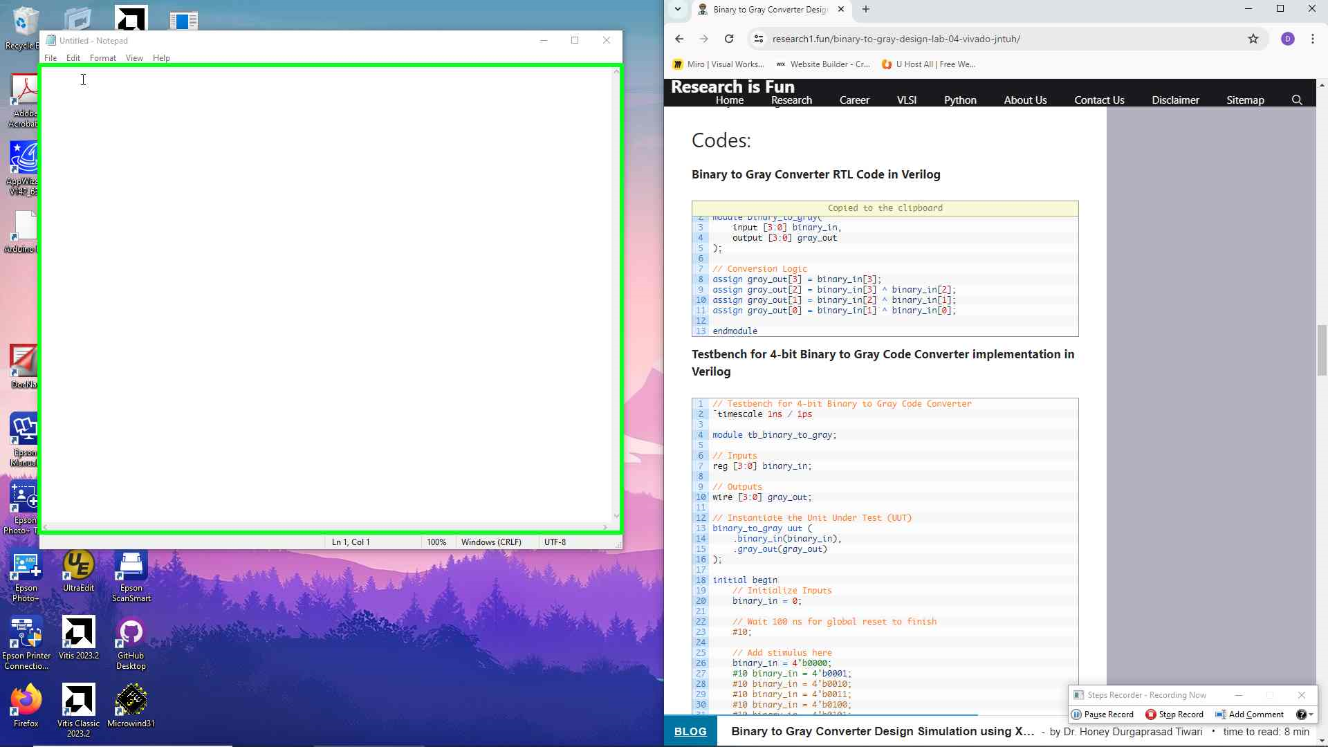
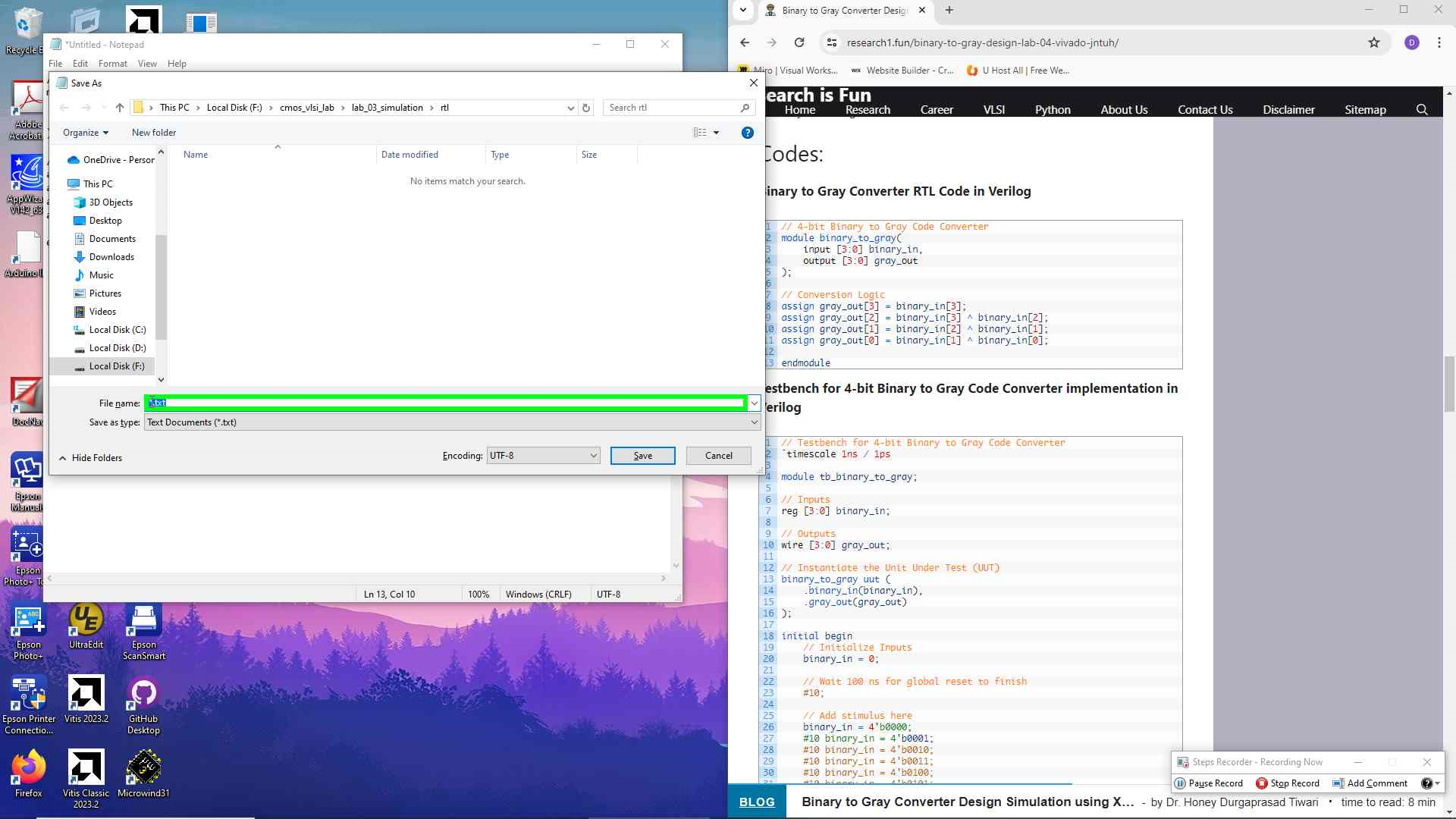
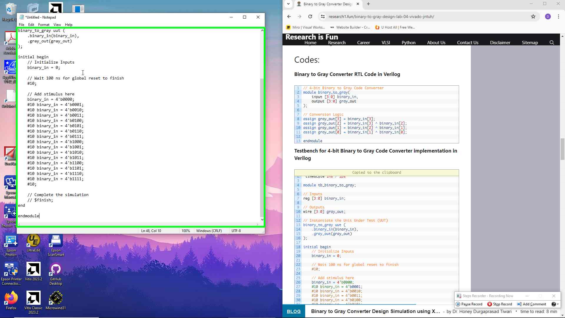
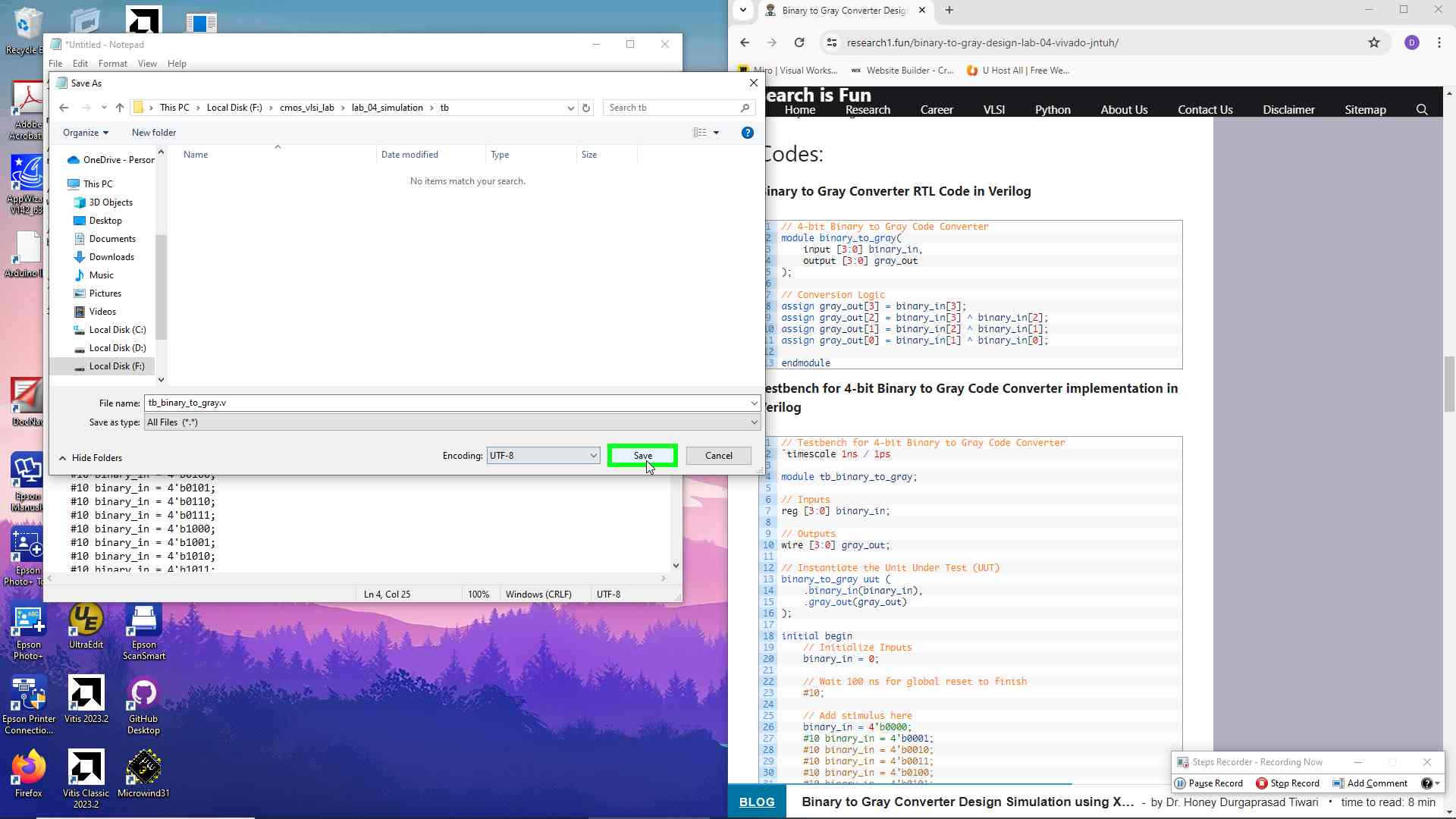
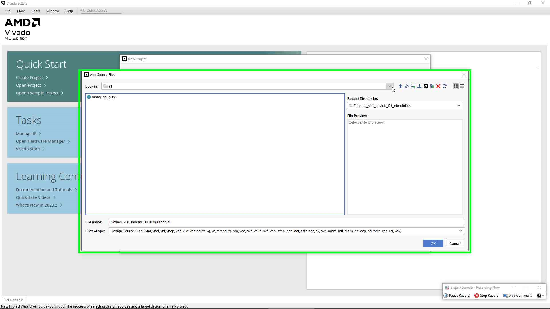
- Open Notepad or any text editor on a Windows machine and write the Verilog code for the 8-to-1 multiplexer and 1-to-8 demultiplexer.
- Save the files with a
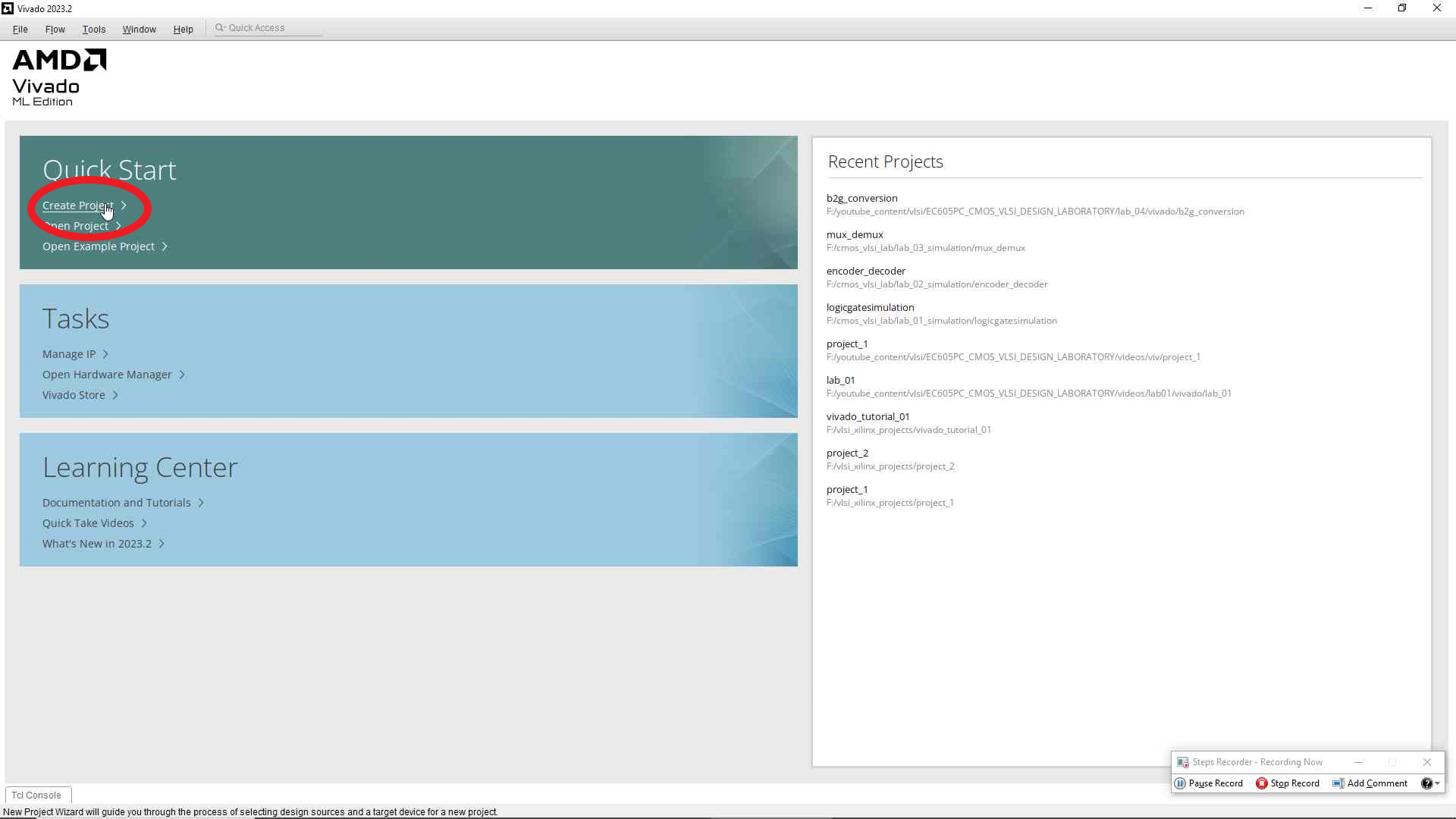
.vextension, selecting “All Files” as the save type. - Launch Xilinx Vivado from the desktop or start menu.
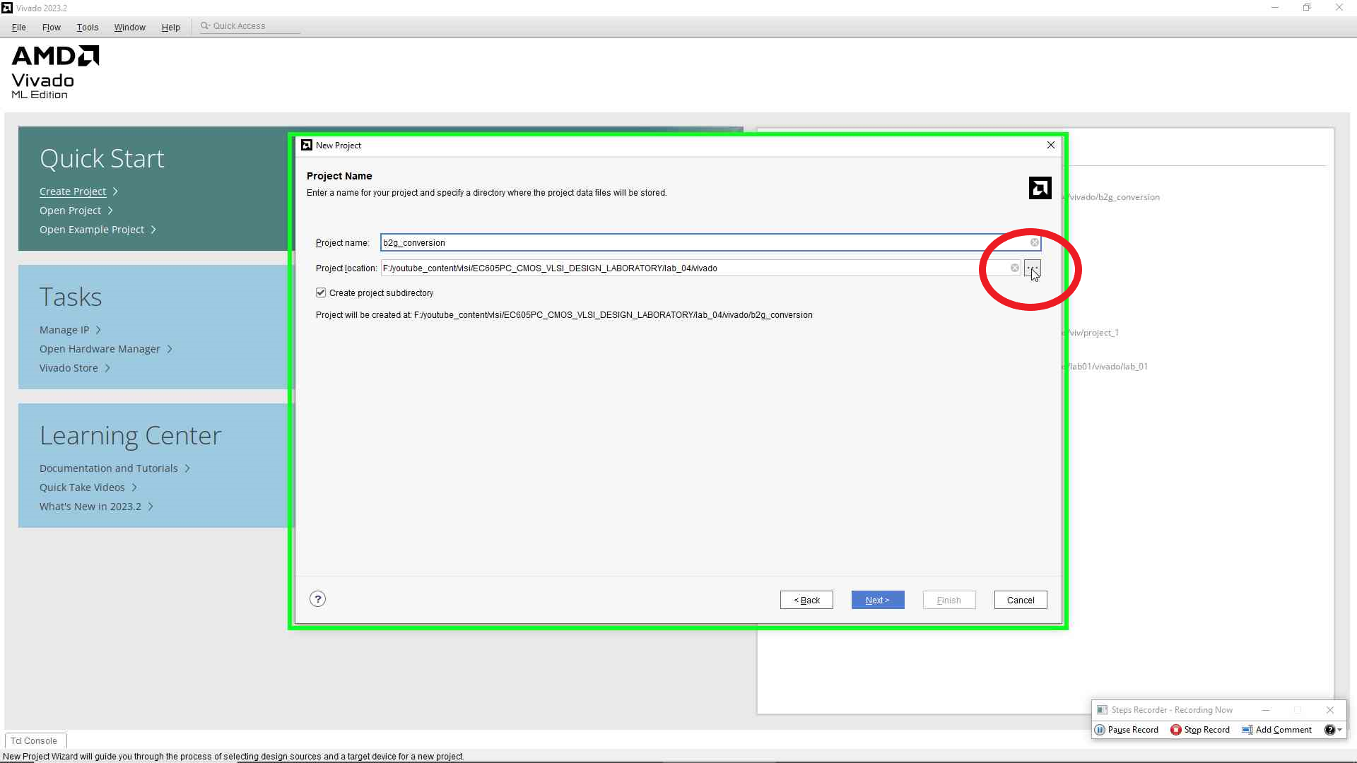
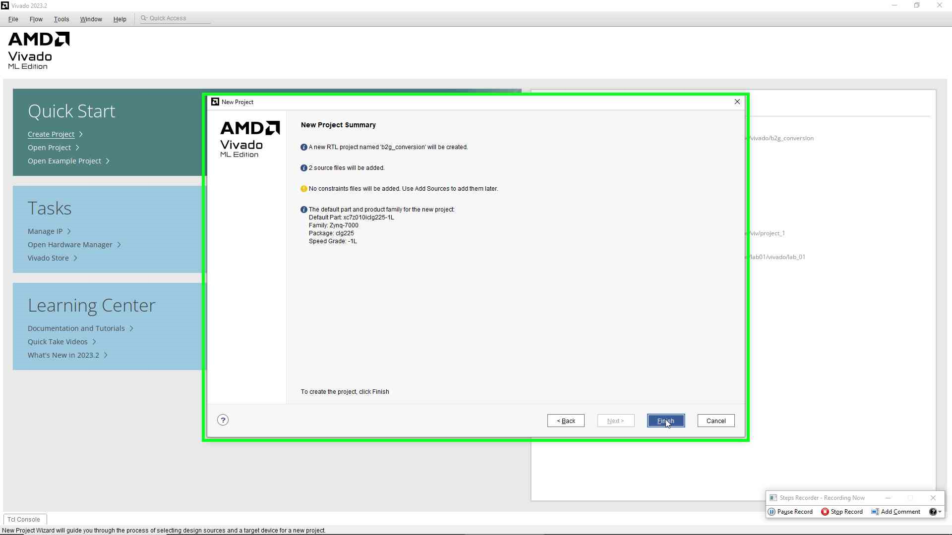
- Create a new project, naming it appropriately (e.g.,
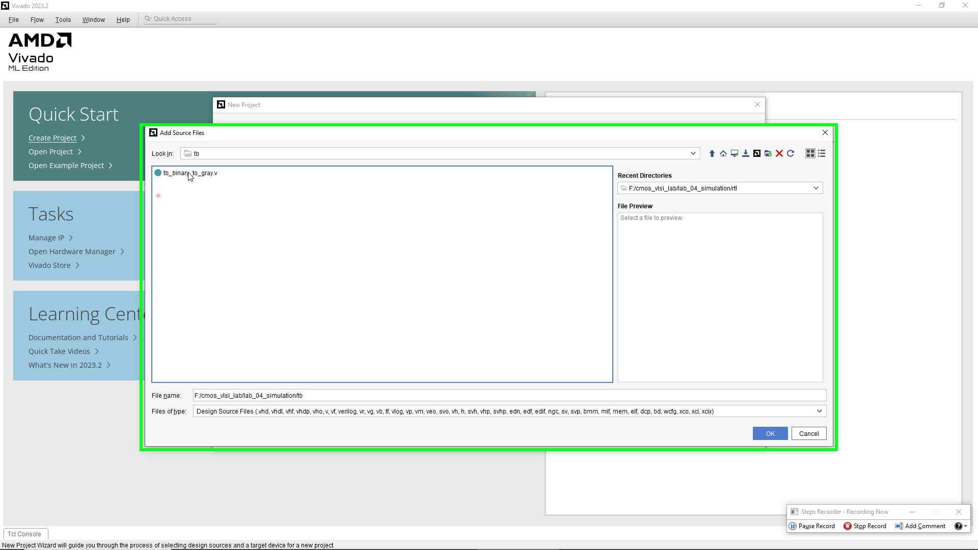
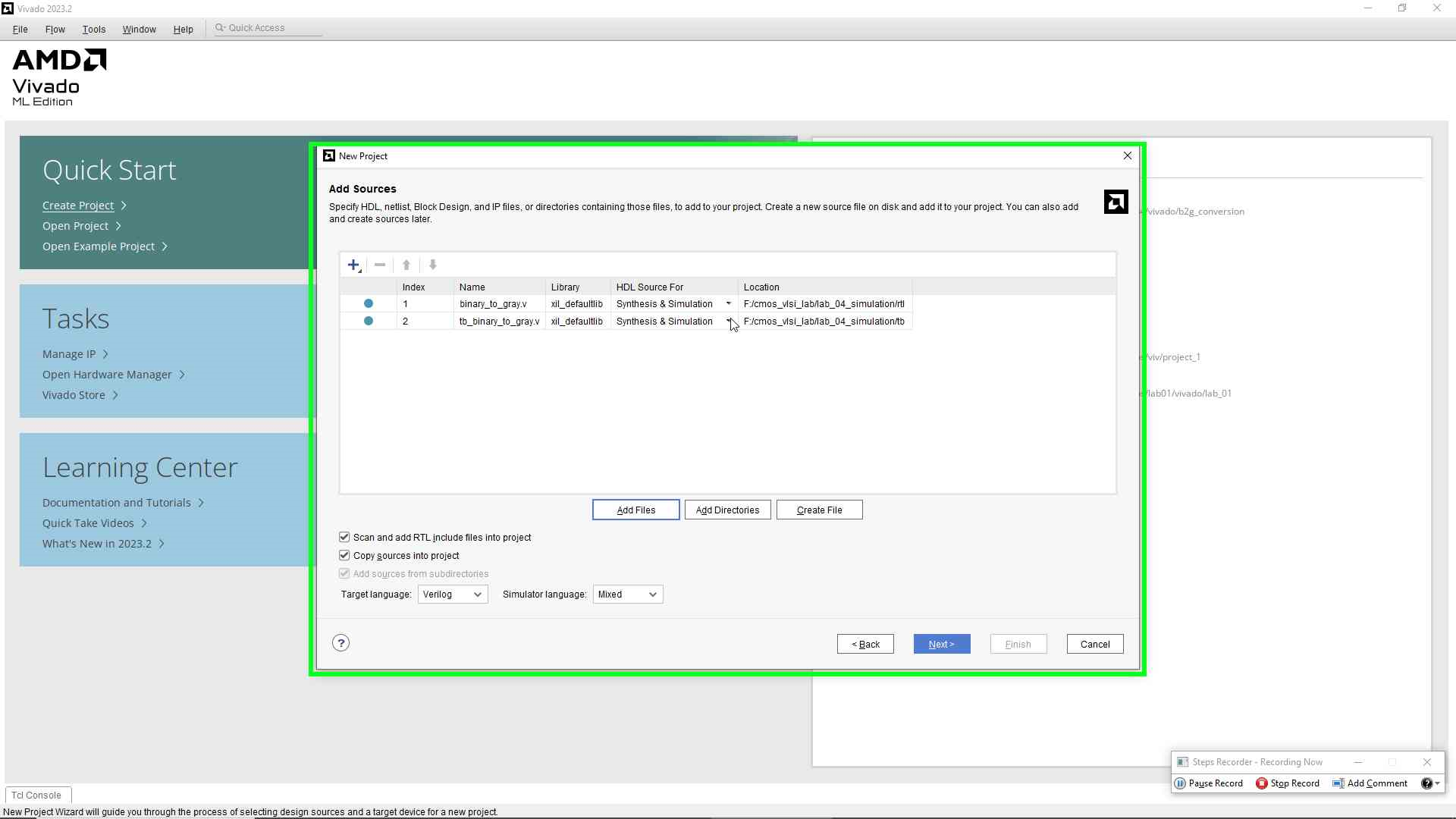
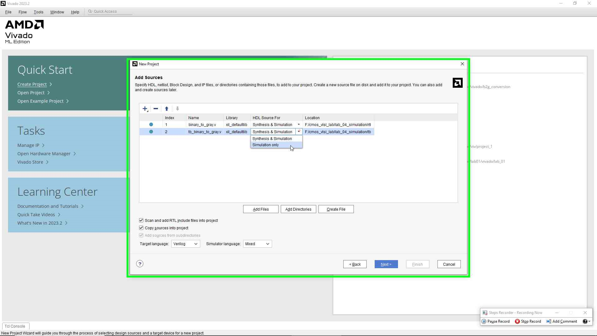
b2g_conversion_lab) and choosing the project’s storage location. - Ensure “RTL Project” is selected and specify sources at this time by pointing to the Verilog source code and testbench files you’ve created.
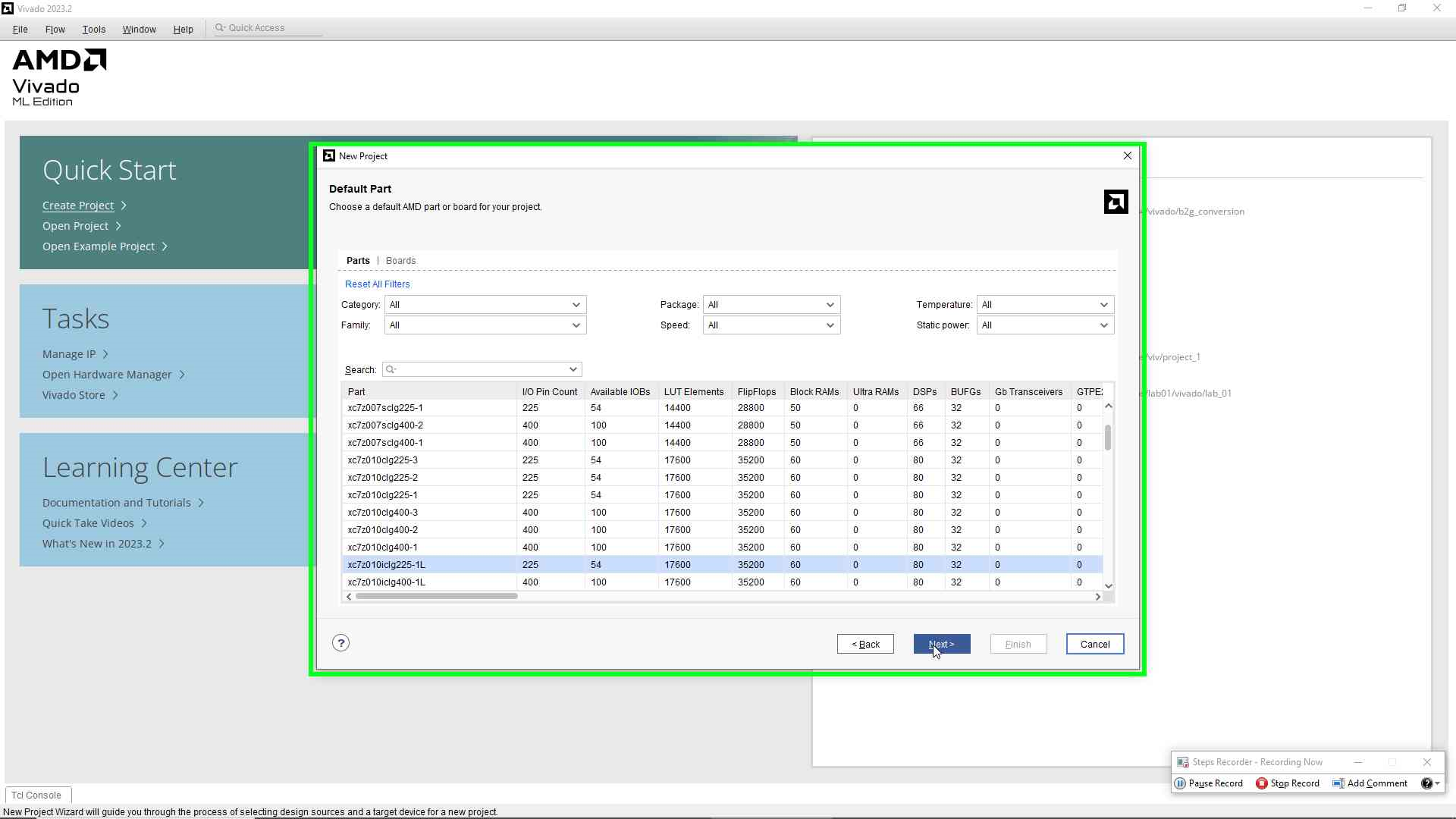
- Select the FPGA board or part targeted for this project using the search function.
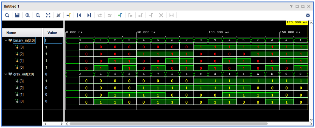
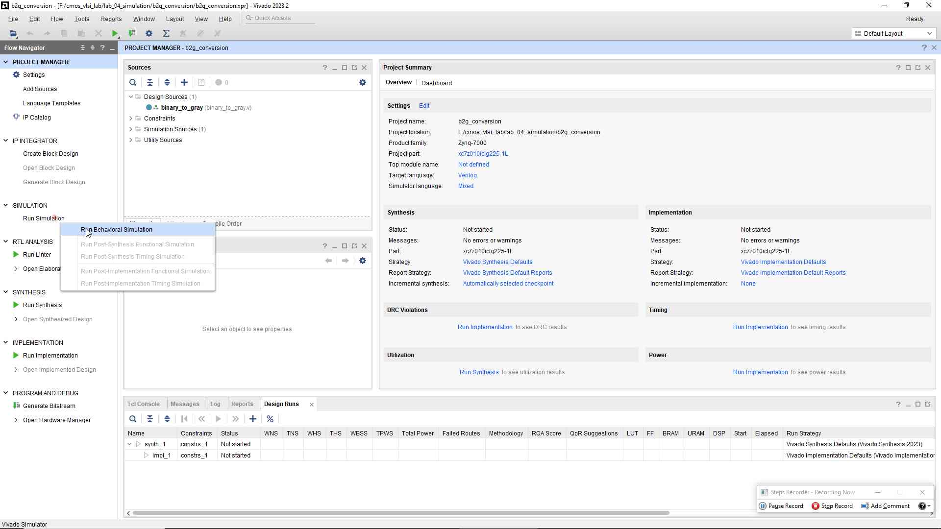
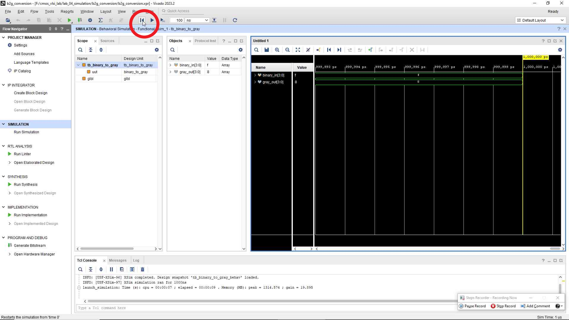
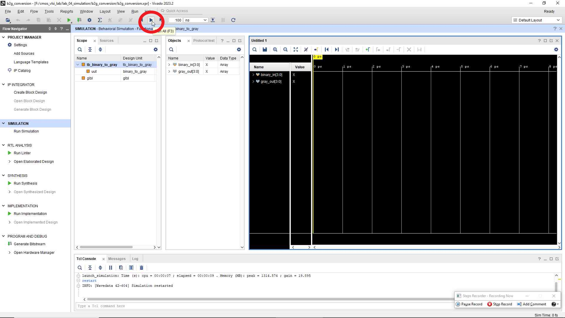
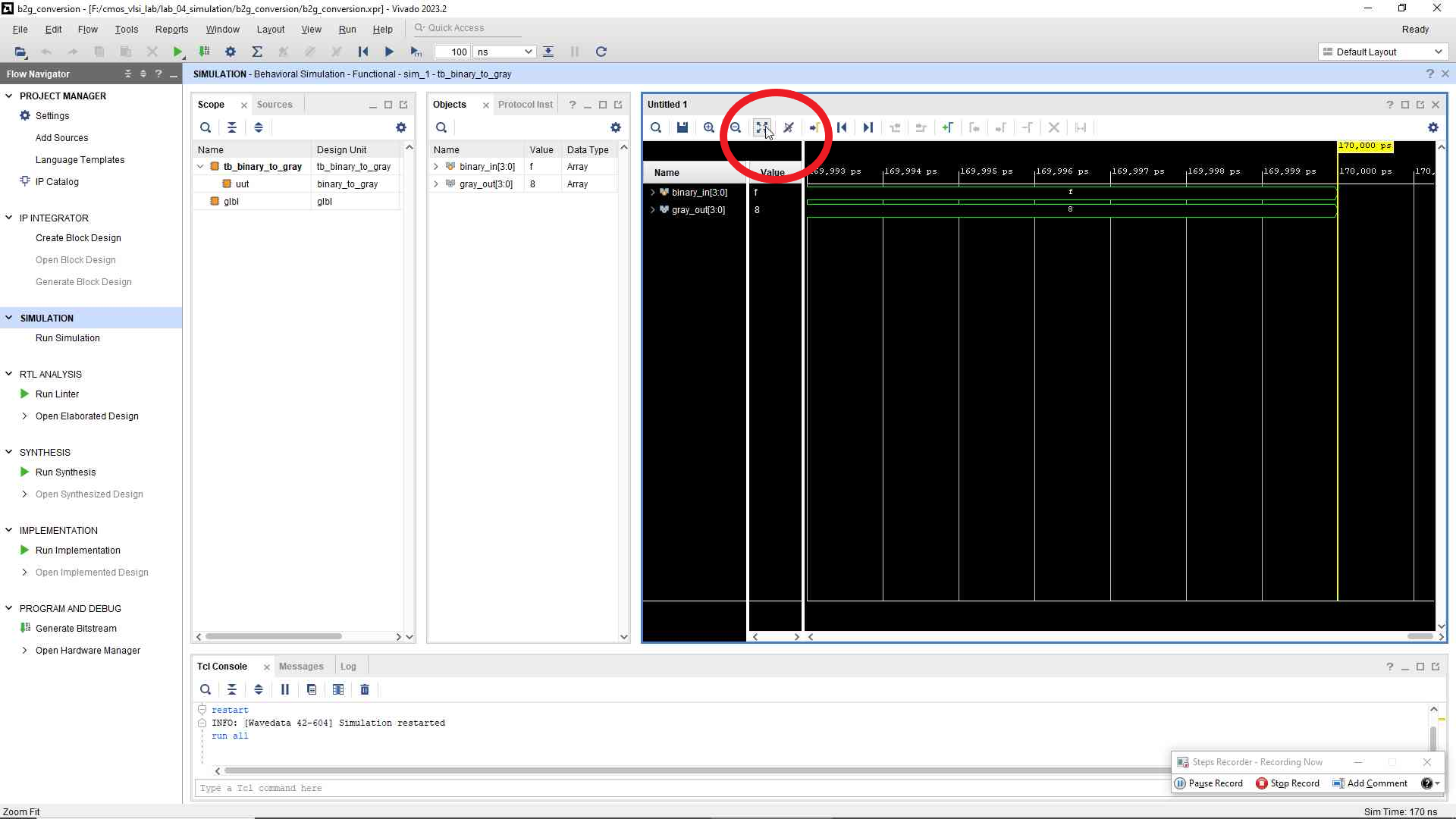
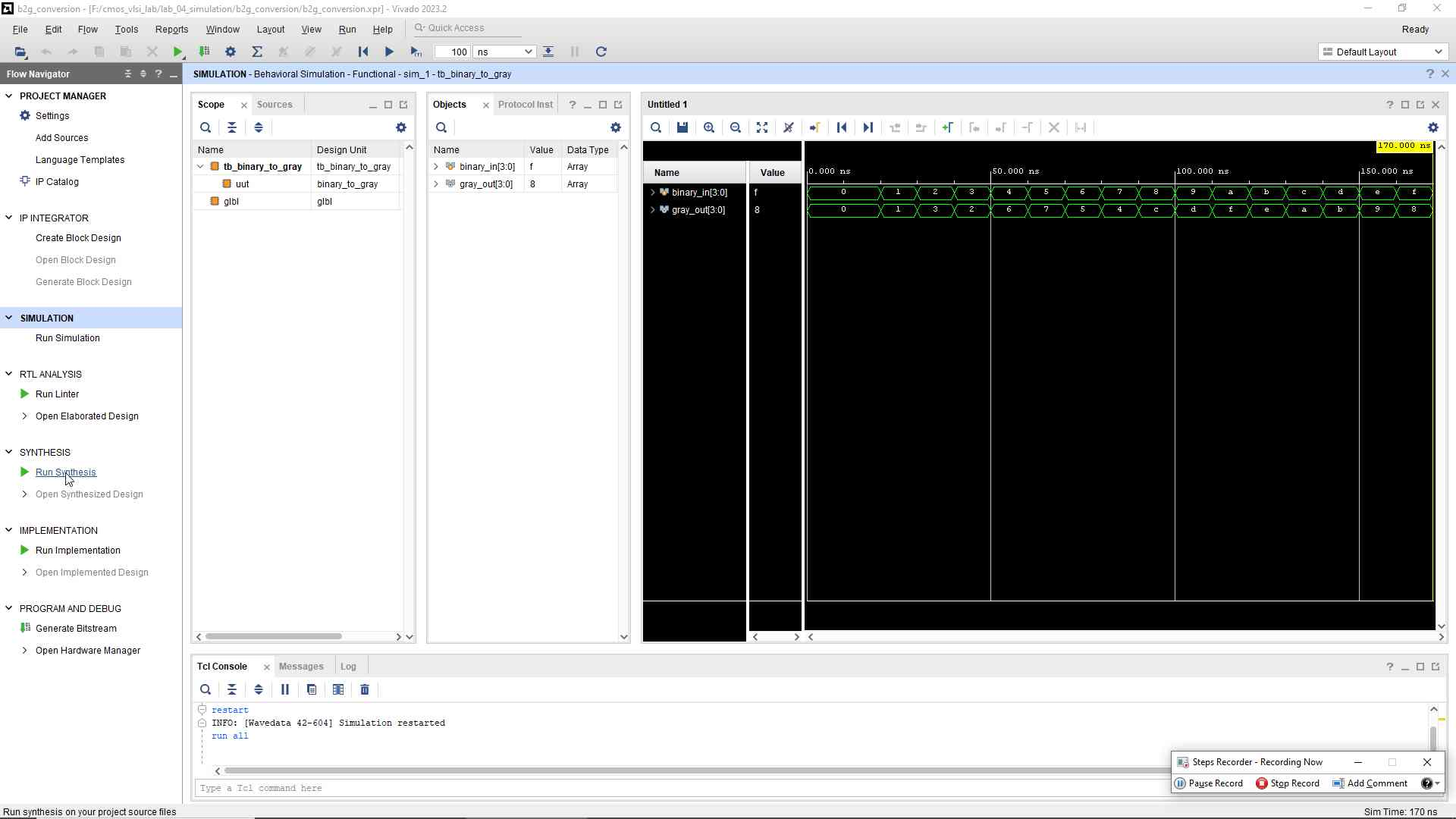
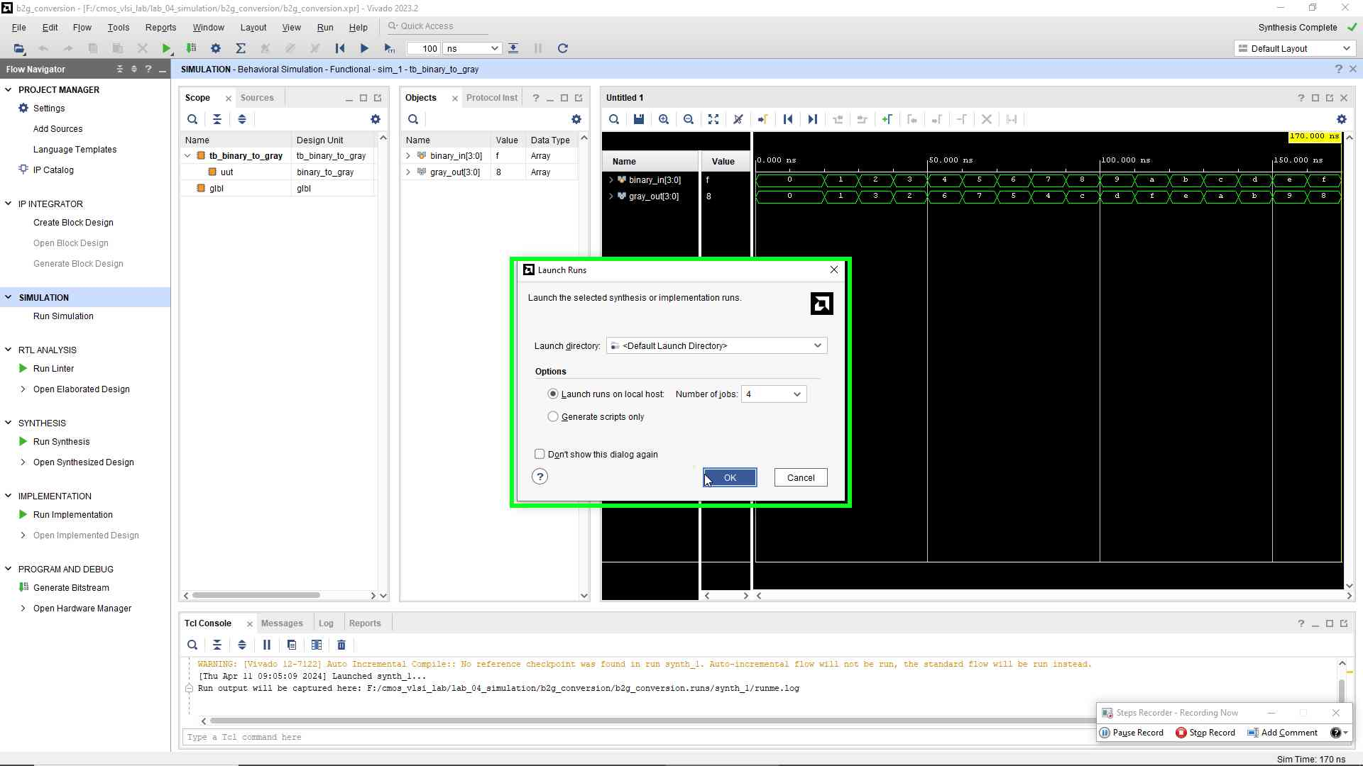
- Run Behavioral Simulation to compile the Verilog files and execute the simulation based on your testbench.
- Inspect the waveform viewer to verify that the outputs match the expected results based on your testbench scenarios.
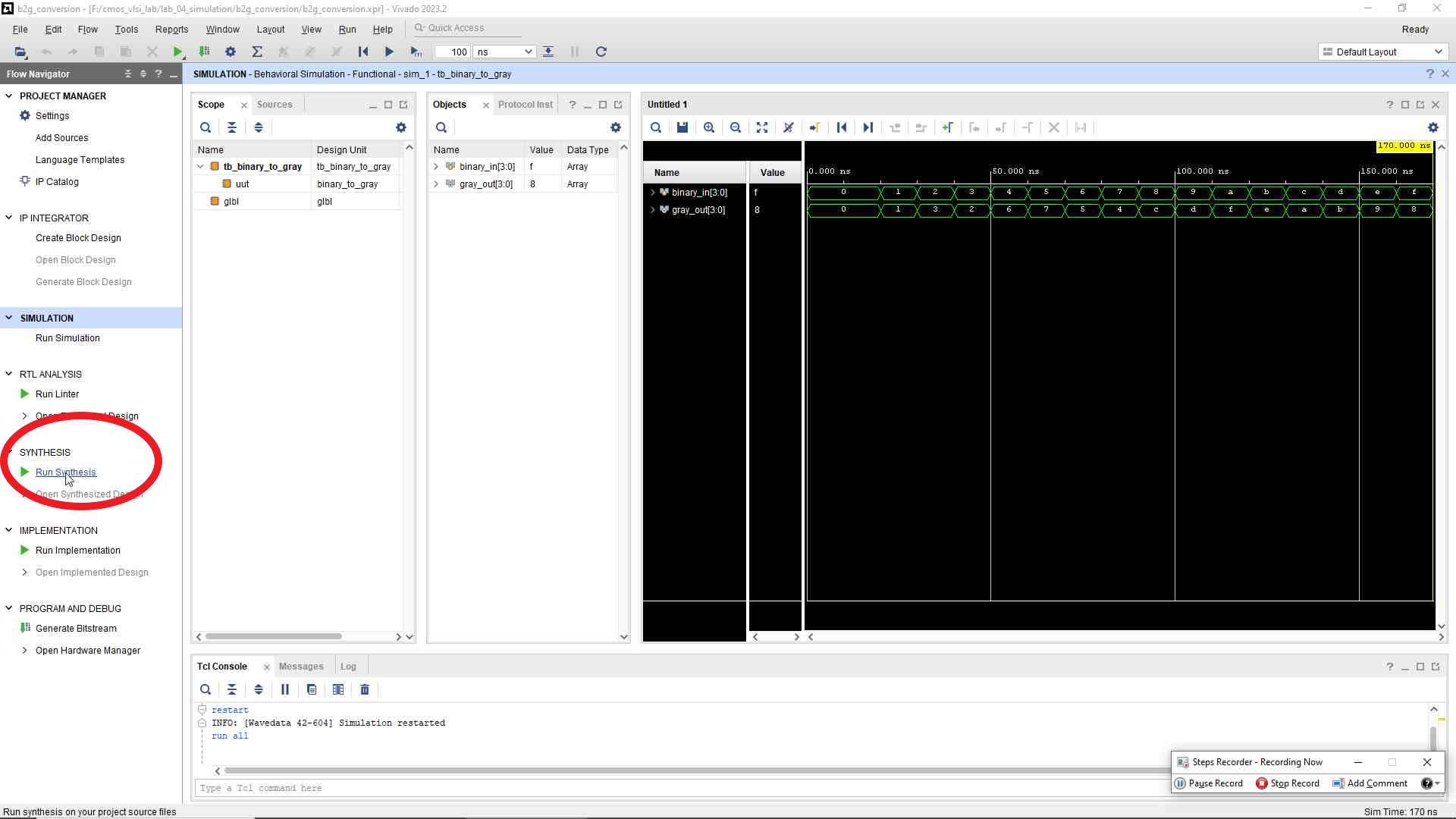
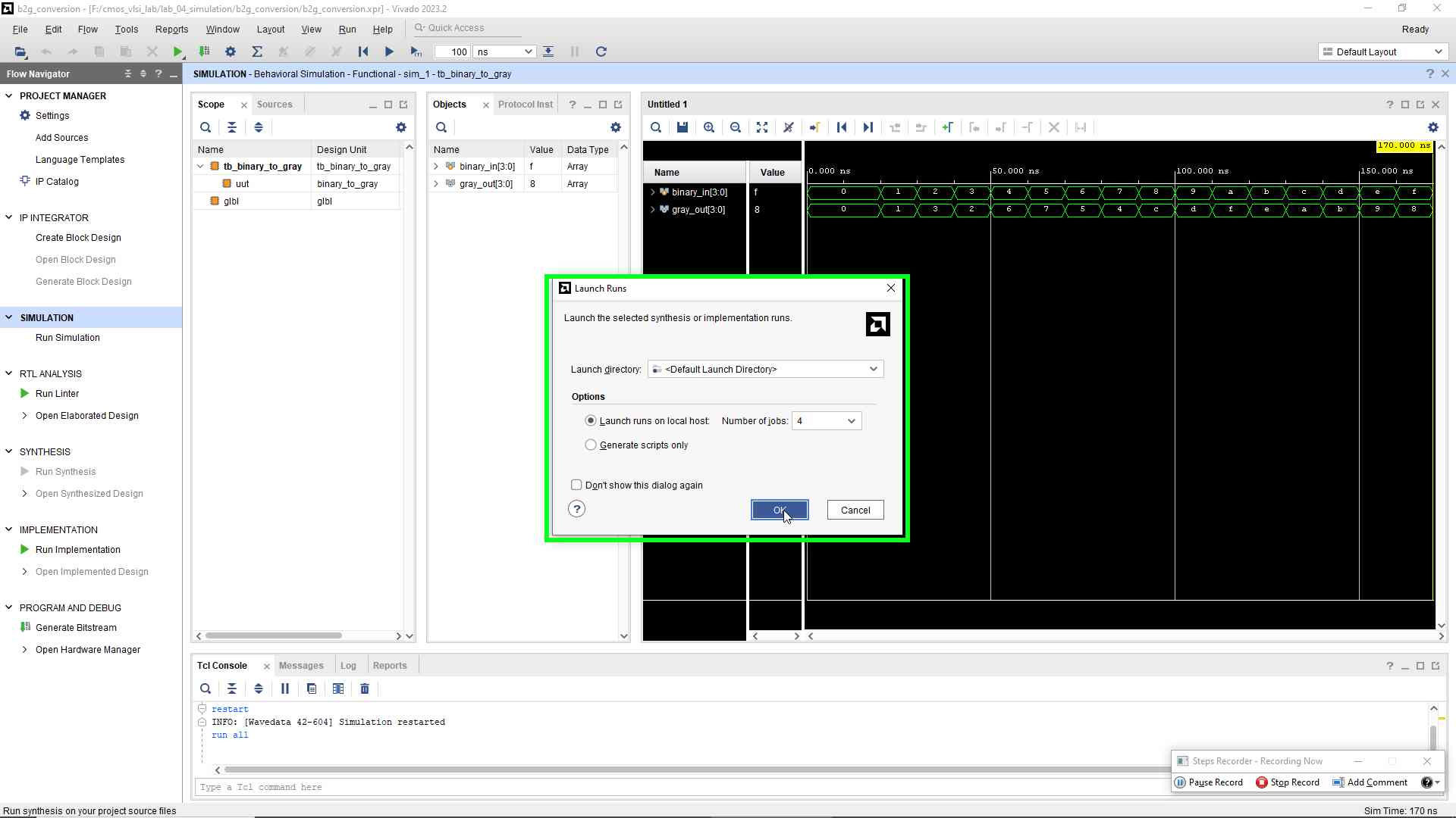
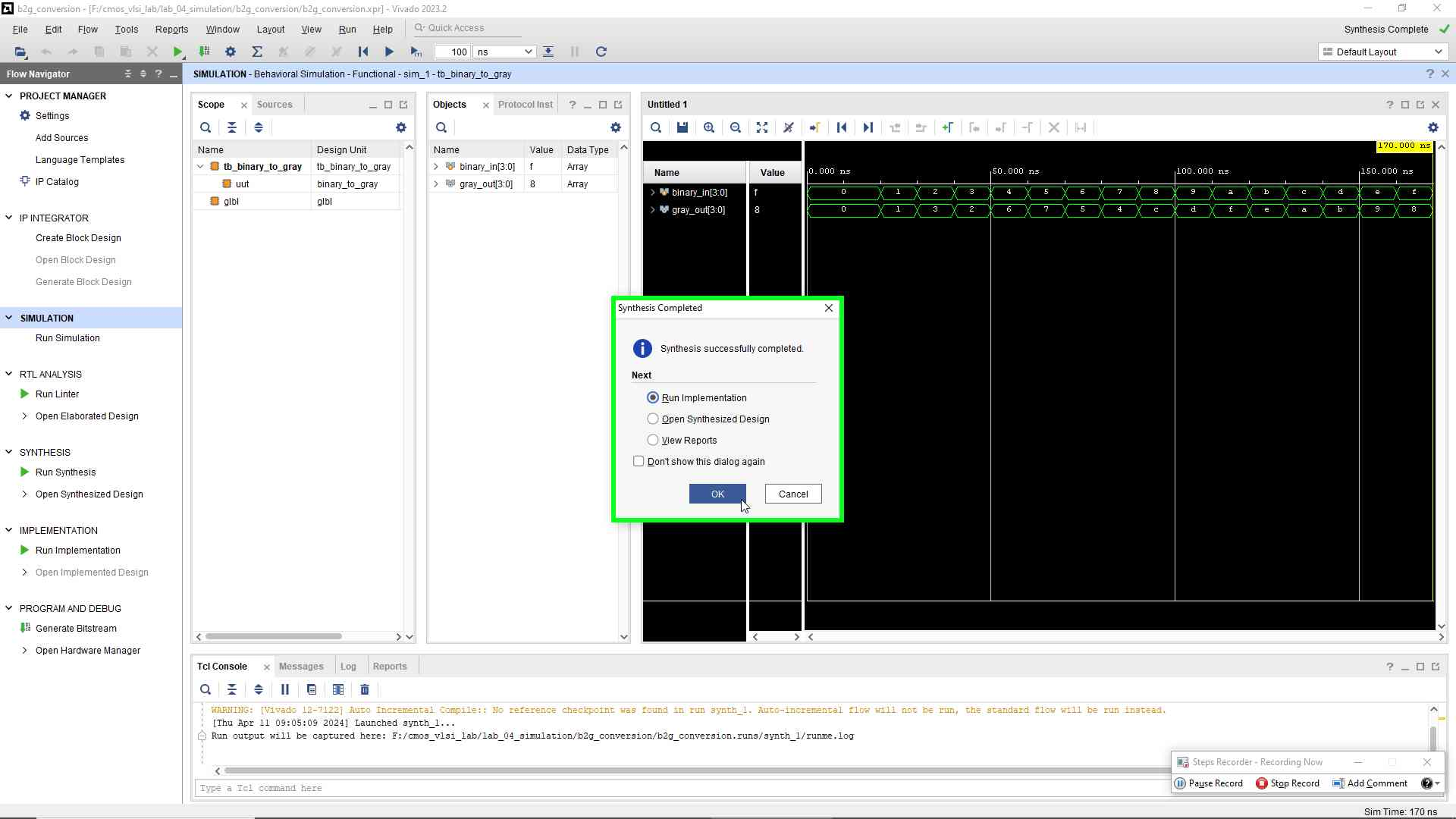
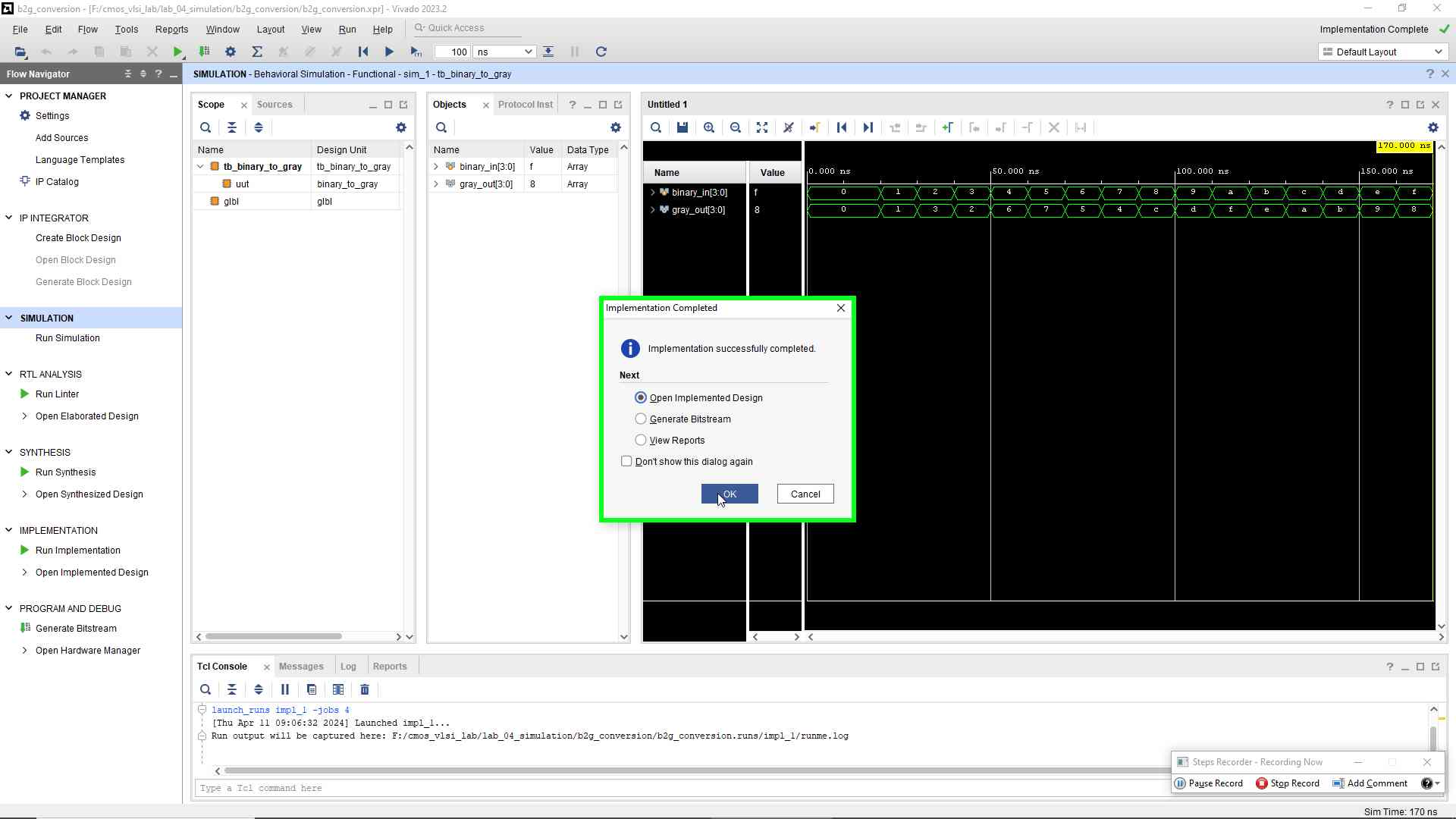
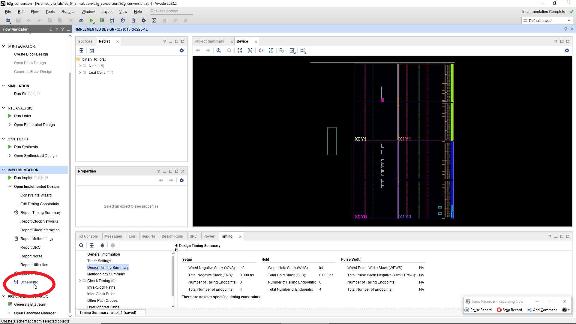
- Proceed with Synthesis and Implementation phases to optimize the design for performance and resource utilization.
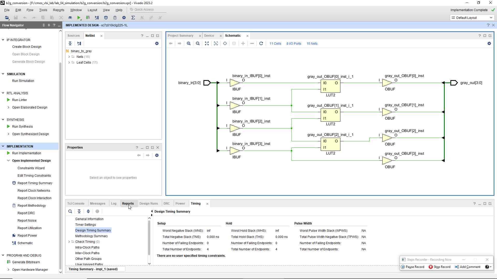
- Analyze the simulation results, synthesized schematic, and implementation reports, making necessary adjustments to refine your design.
Codes:
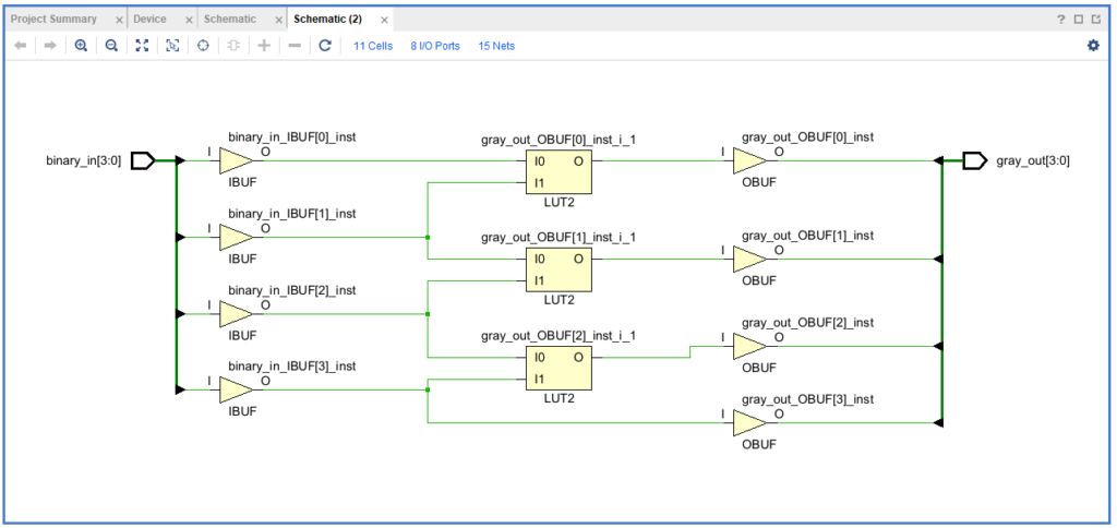
Binary to Gray Converter RTL Code in Verilog
// 4-bit Binary to Gray Code Converter
module binary_to_gray(
    input [3:0] binary_in,
    output [3:0] gray_out
);

// Conversion Logic
assign gray_out[3] = binary_in[3];
assign gray_out[2] = binary_in[3] ^ binary_in[2];
assign gray_out[1] = binary_in[2] ^ binary_in[1];
assign gray_out[0] = binary_in[1] ^ binary_in[0];

endmodule
Testbench for 4-bit Binary to Gray Code Converter implementation in Verilog
// Testbench for 4-bit Binary to Gray Code Converter
`timescale 1ns / 1ps

module tb_binary_to_gray;

// Inputs
reg [3:0] binary_in;

// Outputs
wire [3:0] gray_out;

// Instantiate the Unit Under Test (UUT)
binary_to_gray uut (
    .binary_in(binary_in),
    .gray_out(gray_out)
);

initial begin
    // Initialize Inputs
    binary_in = 0;

    // Wait 100 ns for global reset to finish
    #10;

    // Add stimulus here
    binary_in = 4'b0000;
    #10 binary_in = 4'b0001;
    #10 binary_in = 4'b0010;
    #10 binary_in = 4'b0011;
    #10 binary_in = 4'b0100;
    #10 binary_in = 4'b0101;
    #10 binary_in = 4'b0110;
    #10 binary_in = 4'b0111;
    #10 binary_in = 4'b1000;
    #10 binary_in = 4'b1001;
    #10 binary_in = 4'b1010;
    #10 binary_in = 4'b1011;
    #10 binary_in = 4'b1100;
    #10 binary_in = 4'b1101;
    #10 binary_in = 4'b1110;
    #10 binary_in = 4'b1111;
    #10;

    // Complete the simulation
    // $finish;
end

endmodule
Expected Results:
After following the steps correctly, the simulation in Xilinx Vivado will show the expected behavior for binary to gray conversion, aligning with the input and output relations defined in the theory section.
Conclusion:
This lab experiment solidifies the understanding and application of binaruy to gray convesion in digital design, showcasing the practical use of Xilinx Vivado in simulating complex VLSI components.
Viva-Voce Questions:
- What is the purpose of converting a binary number to Gray code?
- To minimize the possibility of errors during data transfer by ensuring that only one bit changes between consecutive values.
- Can you explain the principle behind the conversion from binary to Gray code?
- The conversion principle involves the most significant bit (MSB) remaining the same, and each subsequent bit being the result of an XOR operation between the adjacent bits of the binary input.
- What is Verilog?
- Verilog is a hardware description language (HDL) used to model electronic systems. It enables the design and testing of digital circuits in a simulation environment.
- Why is Xilinx Vivado used for the synthesis of Verilog designs?
- Xilinx Vivado is an integrated development environment (IDE) that provides tools for the design, simulation, and synthesis of digital circuits, making it suitable for Verilog-based designs.
- How do you define a 4-bit input in Verilog for a binary to Gray code converter?
- A 4-bit input can be defined in Verilog using the syntax
input [3:0] binary;, where[3:0]specifies a 4-bit wide vector.
- A 4-bit input can be defined in Verilog using the syntax
- What is the role of the XOR operation in the conversion from binary to Gray code in your Verilog implementation?
- The XOR operation is used to generate each bit of the Gray code (except for the MSB) by comparing adjacent bits of the binary input, ensuring that only one bit changes at a time.
- Can you describe the test bench used for simulating the binary to Gray code converter in Vivado?
- A test bench in Vivado for this converter would include a module that generates various 4-bit binary inputs, applies them to the converter, and checks the Gray code output for correctness.
- What are some challenges you faced while implementing the converter in Verilog and how did you overcome them?
- This could include debugging syntax errors, ensuring the logic correctly implements the XOR operations, or issues with simulation. Overcoming them typically involves iterative testing and debugging.
- How does the synthesis report in Vivado help in evaluating the performance of the binary to Gray code converter?
- The synthesis report provides details on resource utilization (like logic gates used) and timing information, helping to assess the efficiency and speed of the converter.
- What would be the impact of using a 4-bit binary to Gray code converter in a digital communication system?
- It reduces the risk of errors during data transmission, particularly in scenarios where signal timing might cause multiple bits to change simultaneously if binary encoding were used.
Complete Detailed Procedure for Simulation in Xilinx Vivado
- Preparation: Before opening Vivado, ensure all Verilog source files and testbenches are correctly written and saved.

- Project Creation: Launch Vivado, create a new project, and specify your project’s name and location.

- Adding Files: Include your Verilog source and testbench files in the project setup.

- Selecting Target Device: Choose the FPGA board or part you’re targeting, based on your project requirements.
- Running Simulation: Utilize the Behavioral Simulation feature to compile and simulate your Verilog files.
- Synthesis and Implementation: After verifying the simulation results, proceed with synthesis and implementation to optimize your design.
- Analysis: Review synthesized schematics, implementation reports, and simulation results to ensure the design meets all criteria.
- Adjustments and Finalization: Make any necessary design adjustments based on your analyses and save your project.

Additional Reading:
- FPGA Design Fundamentals
- Verilog for Beginners
- Advanced Digital Design with the Verilog HDL
FAQ
FAQ: Xilinx Vivado
- What is Xilinx Vivado?
- Xilinx Vivado is an integrated development environment (IDE) designed for FPGA (Field Programmable Gate Array) development, offering synthesis, analysis, simulation, and implementation capabilities for digital circuit design.
- How does Vivado differ from ISE (Integrated Synthesis Environment)?
- Vivado is the successor to Xilinx ISE, offering a more modern user interface, improved synthesis and analysis tools, and better support for high-capacity FPGAs. Vivado focuses on newer FPGA architectures like the UltraScale and UltraScale+ series.
- Can Vivado be used for programming in Verilog and VHDL?
- Yes, Vivado supports both Verilog and VHDL for designing digital circuits, allowing users to simulate, synthesize, and implement designs using either hardware description language.
- Is there a free version of Vivado available?
- Yes, Xilinx offers a Vivado Design Suite WebPACK Edition, which is free and includes enough features for students, hobbyists, and researchers to design and program FPGAs.
- What are the system requirements for installing Vivado?
- Vivado requires a Windows or Linux operating system with specific hardware requirements, including a 64-bit processor, at least 8 GB of RAM (32 GB recommended for large designs), and around 20 GB of free disk space for installation.
- How can I learn to use Vivado?
- Xilinx offers comprehensive documentation, tutorials, and video training courses for Vivado. Many universities and online platforms also provide courses and materials on FPGA design using Vivado.
- What is the role of the Vivado High-Level Synthesis (HLS)?
- Vivado HLS allows designers to write C, C++, or SystemC code to describe their hardware functions, which Vivado HLS then synthesizes into optimized VHDL/Verilog code, enabling a higher level of abstraction in design.
- Can I simulate my FPGA design without a physical board using Vivado?
- Yes, Vivado includes a simulator that allows you to test and debug your FPGA designs thoroughly before deploying them to actual hardware.
- How does Vivado manage version control and collaborative work?
- Vivado integrates with version control systems like Git and Subversion, enabling teams to collaborate on projects efficiently. It also supports project sharing and IP (Intellectual Property) reuse to facilitate teamwork.
- What kind of support does Xilinx offer for Vivado users?
- Xilinx provides a range of support options for Vivado users, including detailed documentation, a user community forum, technical support for licensed users, and training programs for both beginners and advanced users.
Reference:
- Official Xilinx Vivado Documentation
- Digital Design and Computer Architecture by Harris & Harris
- FPGA Prototyping by Verilog Examples by Pong P. Chu
Here are the reference links formatted for inclusion in your blog:
Internal Links:
- JNTUH VLSI Lab Experiments – Explore a series of lab experiments for understanding VLSI design concepts using Xilinx Vivado.
CMOS VLSI LAB CYCLE 01:
Lab Reports and Related YouTube Videos:
- Lab 01: Logic Gates
- Lab 02: Encoder and Decoder
- Lab 03: Multiplexer, Demultiplexer
CMOS VLSI LAB CYCLE 02:
Lab Reports and Related YouTube Video:
- Lab 01 Part-2: Basic Logic Gates Layout