Encoder / Decoder Design Lab Manual
AIM:
To design and simulate 8-to-3 encoder (without and with priority) and 2-to-4 decoder using Xilinx Vivado.
Apparatus / Software required:
- Xilinx Vivado 2023.2
- PC with Windows Operating System
- Verilog files for encoder and decoder
Theory:
In digital electronics, an encoder is a device that converts data from one format to another for standardization, speed, or compression. An 8-to-3 encoder without priority encodes eight inputs into three outputs, while the version with priority considers the highest priority input. A 2-to-4 decoder does the opposite, decoding the information from 2 inputs back into 4 outputs.
Encoder (8-to-3) without priority:
| Input | D7 | D6 | D5 | D4 | D3 | D2 | D1 | D0 | Output | Y2 | Y1 | Y0 |
|---|---|---|---|---|---|---|---|---|---|---|---|---|
| 0 | 0 | 0 | 0 | 0 | 0 | 0 | 1 | 0 | 0 | 0 | ||
| 0 | 0 | 0 | 0 | 0 | 0 | 1 | X | 0 | 0 | 1 | ||
| 0 | 0 | 0 | 0 | 0 | 1 | X | X | 0 | 1 | 0 | ||
| 0 | 0 | 0 | 0 | 1 | X | X | X | 0 | 1 | 1 | ||
| 0 | 0 | 0 | 1 | X | X | X | X | 1 | 0 | 0 | ||
| 0 | 0 | 1 | X | X | X | X | X | 1 | 0 | 1 | ||
| 0 | 1 | X | X | X | X | X | X | 1 | 1 | 0 | ||
| 1 | X | X | X | X | X | X | X | 1 | 1 | 1 |
Encoder (8-to-3) with priority:
The complete table for an Encoder (8-to-3) with priority is given below. This table assumes that when multiple inputs are active, the input with the highest priority (D7 being the highest and D0 the lowest) will determine the output, regardless of the state of the lower-priority inputs.
| Inputs | D7 | D6 | D5 | D4 | D3 | D2 | D1 | D0 | Output | Y2 | Y1 | Y0 |
|---|---|---|---|---|---|---|---|---|---|---|---|---|
| Case 1 | 1 | X | X | X | X | X | X | X | 1 | 1 | 1 | |
| Case 2 | 0 | 1 | X | X | X | X | X | X | 1 | 1 | 0 | |
| Case 3 | 0 | 0 | 1 | X | X | X | X | X | 1 | 0 | 1 | |
| Case 4 | 0 | 0 | 0 | 1 | X | X | X | X | 1 | 0 | 0 | |
| Case 5 | 0 | 0 | 0 | 0 | 1 | X | X | X | 0 | 1 | 1 | |
| Case 6 | 0 | 0 | 0 | 0 | 0 | 1 | X | X | 0 | 1 | 0 | |
| Case 7 | 0 | 0 | 0 | 0 | 0 | 0 | 1 | X | 0 | 0 | 1 | |
| Case 8 | 0 | 0 | 0 | 0 | 0 | 0 | 0 | 1 | 0 | 0 | 0 |
In this table:
- “X” denotes a “don’t care” condition where the value can be either 0 or 1. This reflects the priority logic, where the output is determined solely by the highest priority input that is active.
- The Output columns (Y2, Y1, Y0) represent the binary output of the encoder based on which input is active. For example, if D7 is active (Case 1), the output is 111 regardless of the states of D6 to D0.
Decoder (2-to-4):
| Input | Y1 | Y0 | Output | D3 | D2 | D1 | D0 |
|---|---|---|---|---|---|---|---|
| 0 | 0 | 0 | 0 | 0 | 1 | ||
| 0 | 1 | 0 | 0 | 1 | 0 | ||
| 1 | 0 | 0 | 1 | 0 | 0 | ||
| 1 | 1 | 1 | 0 | 0 | 0 |
Procedure:
- Launch Xilinx Vivado: Start by opening Xilinx Vivado 2023.2 on your computer.
- Create a New Project: Select “File” > “New Project.” Follow the wizard to name your project and select the appropriate directory.
- Add Source Files: Choose “Add or create design sources” and include the Verilog files (
encoder_8to3.v,encoder_8to3_priority.v, anddecoder_2to4.v) for your encoders and decoder. - Add Testbench: Add the
tb_encoder_decoder.vfile to your project to test the encoder and decoder designs. - Set Up Simulation: Navigate to the “Flow Navigator” and select “Run Simulation” > “Run Behavioral Simulation.”
- Observe the Results: Review the waveforms in the simulation results to verify the functionality of your encoder and decoder designs against expected outcomes.
- Analyze and Save: Analyze the performance and functionality of your designs. Make adjustments as needed and save your project.
Codes
8-to-3 Encoder without Priority Verilog Code
// 8-to-3 Encoder without Priority
module encoder_8to3(input wire [7:0] in, output reg [2:0] out);
    always @(in) begin
        case (in)
            8'b00000001: out = 3'b000;
            8'b00000010: out = 3'b001;
            8'b00000100: out = 3'b010;
            8'b00001000: out = 3'b011;
            8'b00010000: out = 3'b100;
            8'b00100000: out = 3'b101;
            8'b01000000: out = 3'b110;
            8'b10000000: out = 3'b111;
            default: out = 3'bZZZ; // When multiple inputs are high
        endcase
    end
endmodule
8-to-3 Encoder with Priority
// 8-to-3 Encoder with Priority
module encoder_8to3_priority(input wire [7:0] in, output reg [2:0] out);
    always @(in) begin
        casex (in)
            8'b1xxxxxxx: out = 3'b111;
            8'b01xxxxxx: out = 3'b110;
            8'b001xxxxx: out = 3'b101;
            8'b0001xxxx: out = 3'b100;
            8'b00001xxx: out = 3'b011;
            8'b000001xx: out = 3'b010;
            8'b0000001x: out = 3'b001;
            8'b00000001: out = 3'b000;
            default: out = 3'bZZZ; // When no inputs are high
        endcase
    end
endmodule
2-to-4 Decoder
// 2-to-4 Decoder
module decoder_2to4(input wire [1:0] in, output reg [3:0] out);
    always @(in) begin
        case(in)
            2'b00: out = 4'b0001;
            2'b01: out = 4'b0010;
            2'b10: out = 4'b0100;
            2'b11: out = 4'b1000;
            default: out = 4'b0000;
        endcase
    end
endmodule
Testbench for 8-to-3 Encoder (without and with priority) and 2-to-4 Decoder
// Testbench for 8-to-3 Encoder (without and with priority) and 2-to-4 Decoder
`timescale 1ns / 1ps
module tb_encoder_decoder;
    reg [7:0] in_encoder;
    reg [1:0] in_decoder;
    wire [2:0] out_encoder, out_encoder_priority;
    wire [3:0] out_decoder;

    // Instantiate the modules
    encoder_8to3 enc(in_encoder, out_encoder);
    encoder_8to3_priority enc_p(in_encoder, out_encoder_priority);
    decoder_2to4 dec(in_decoder, out_decoder);

    initial begin
        // Test cases for encoders and decoder
        in_encoder = 8'b00000001; in_decoder = 2'b00; #10;
        in_encoder = 8'b00001000; in_decoder = 2'b01; #10;
        in_encoder = 8'b10000000; in_decoder = 2'b10; #10;
        in_encoder = 8'b00010000; in_decoder = 2'b11; #10;
        in_encoder = 8'b00000011; in_decoder = 2'b00; #10;
        in_encoder = 8'b00001100; in_decoder = 2'b01; #10;
        in_encoder = 8'b10000001; in_decoder = 2'b10; #10;
        in_encoder = 8'b10010001; in_decoder = 2'b11; #10;
        // $finish;
    end
endmodule
Results:
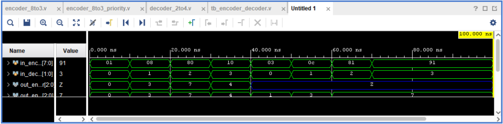
The simulation in Vivado will demonstrate the functionality of both encoders and the decoder as described in the theory section.
Conclusion:
The lab successfully simulates the operation of 8-to-3 encoders (with and without priority) and a 2-to-4 decoder using Xilinx Vivado, providing a practical understanding of digital encoding and decoding processes.
Viva-Voce Questions:
- What does a 2-to-4 decoder do?
A: A 2-to-4 decoder converts 2-bit inputs into one of four outputs, each corresponding to one of the input combinations. - Why is priority given in encoders?
A: Priority is given to ensure that when multiple inputs are active, the highest-priority input is recognized and encoded. - How does Vivado assist in VLSI design?
A: Vivado facilitates design entry, synthesis, implementation, and simulation of VLSI designs, providing an integrated environment for development. - What is the significance of the test bench in simulation?
A: The test bench provides a controlled environment to simulate and verify the functionality of digital designs by applying test vectors. - Can you explain the difference between synthesis and simulation?
A: Synthesis translates high-level design descriptions (HDL) into gate-level or netlist form. Simulation, however, tests the behavior of the design under various conditions without physical realization. - Why are Verilog and VHDL used in digital design?
A: Verilog and VHDL are hardware description languages used to model and describe the structure and behavior of electronic systems at various levels of abstraction. - What role does the ‘Run Behavioral Simulation’ play in Vivado?
A: It simulates the design’s behavior based on the written HDL code, allowing designers to verify functionality and timing without physical hardware. - How do you interpret the waveforms in Vivado simulation?
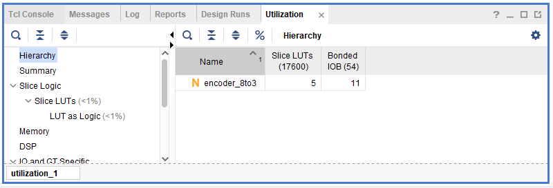
A: Waveforms in Vivado show the logical states (0 or 1) of signals over time, helping analyze the temporal behavior and interactions between different signals. - What is the purpose of the ‘Report Utilization’ feature in Vivado?
A: It provides detailed information on resource usage within the FPGA, such as the number of utilized LUTs, registers, and IOs, aiding in the optimization of the design. - What is the significance of choosing a specific FPGA board for a project in Vivado?
A: The choice of FPGA board determines the available resources (LUTs, IO pins, memory) for the project, affecting how the design is implemented and optimized for specific hardware constraints.
Complete detailed procedure in details for simulation in Xilinx Vivado
Step One: Launching Vivado
- Open Xilinx Vivado by clicking on its icon from your desktop or start menu.
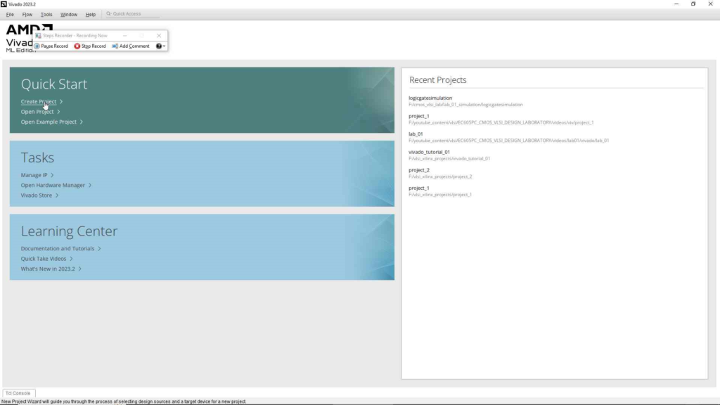
Step Two: Creating a New Project
- Once Vivado is open, click on “File” > “New Project” to start a new project setup wizard.
- Press “Next” on the introductory dialog box.

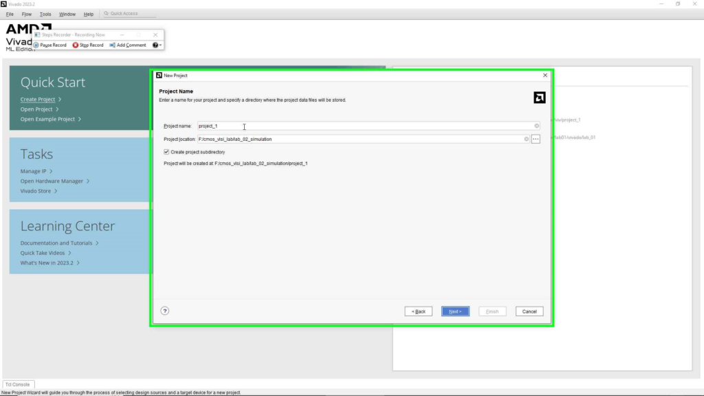
Step Three: Project Name and Location
- Assign a name to your project, such as “encoder_decoder”, and specify the location where the project will be stored.
- Click “Next” to proceed.
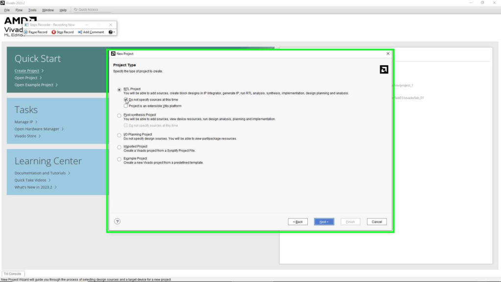
Step Four: Project Type
- Ensure “RTL Project” is selected. Confirm that “Do not specify sources at this time” is checked since we’ll be creating new source files directly in Vivado.
- Click “Next”.
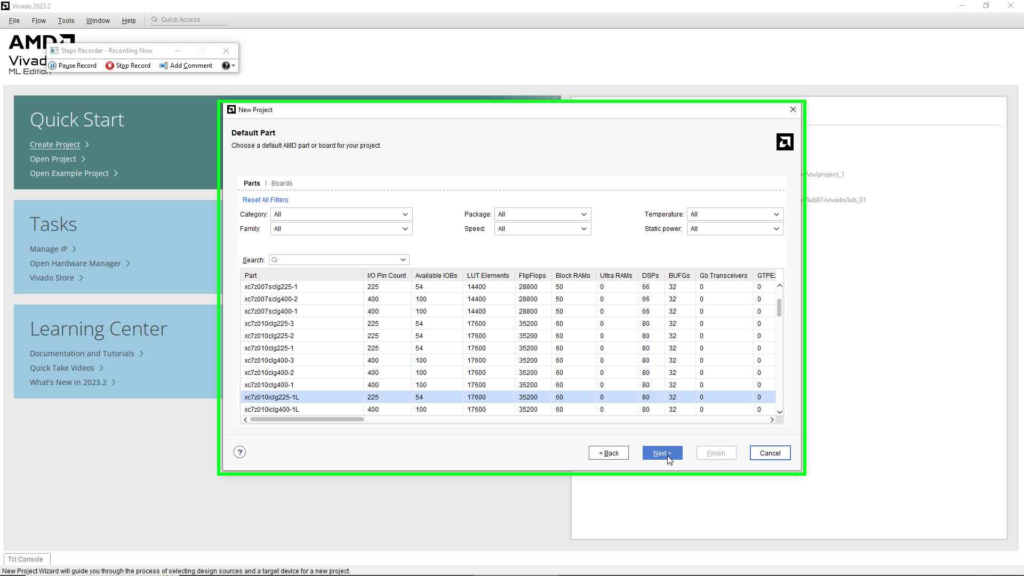
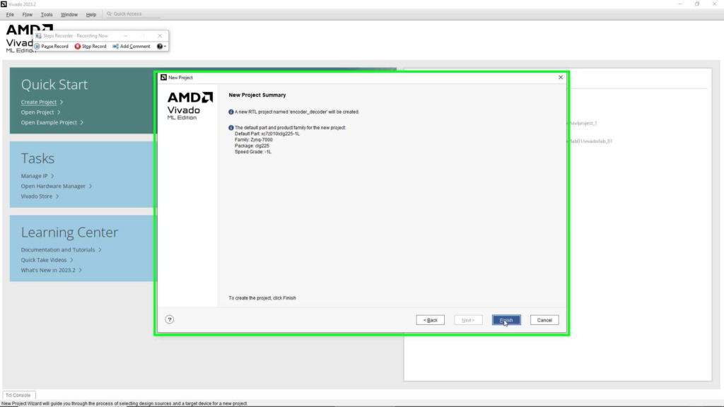
Step Five: Default Part Selection
- In the “Default Part” screen, select the FPGA board or part you will be targeting for this project. You can use the filters or search function to easily find your device.
- Click “Next” after making your selection, then “Finish” to create your new project.
Step Six: Creating Verilog Source Files
- In the Project Manager, right-click on “Design Sources” and select “Add Sources”.
- Choose “Add or create design sources” and then click “Create File”.
- Enter the file name for your first Verilog source, such as “encoder_8to3.v”, set the file type to “Verilog”, and click “OK”. Repeat this process for additional files: “encoder_8to3_priority.v”, “decoder_2to4.v”.
- For each created file, input the Verilog code directly into the Vivado editor that opens for each file. Save your progress.
[su_image_carousel source=”media: 875″ limit=”1″ captions=”yes” arrows=”no” dots=”no” link=”none” target=”blank” autoplay=”0″ image_size=”full” prefer_caption=”yes”]
[su_image_carousel source=”media: 876″ limit=”1″ captions=”yes” arrows=”no” dots=”no” link=”none” target=”blank” autoplay=”0″ image_size=”full” prefer_caption=”yes”]
[su_image_carousel source=”media: 877″ limit=”1″ captions=”yes” arrows=”no” dots=”no” link=”none” target=”blank” autoplay=”0″ image_size=”full” prefer_caption=”yes”]
[su_image_carousel source=”media: 878″ limit=”1″ captions=”yes” arrows=”no” dots=”no” link=”none” target=”blank” autoplay=”0″ image_size=”full” prefer_caption=”yes”]
[su_image_carousel source=”media: 879″ limit=”1″ captions=”yes” arrows=”no” dots=”no” link=”none” target=”blank” autoplay=”0″ image_size=”full” prefer_caption=”yes”]
[su_image_carousel source=”media: 880″ limit=”1″ captions=”yes” arrows=”no” dots=”no” link=”none” target=”blank” autoplay=”0″ image_size=”full” prefer_caption=”yes”]
[su_image_carousel source=”media: 881″ limit=”1″ captions=”yes” arrows=”no” dots=”no” link=”none” target=”blank” autoplay=”0″ image_size=”full” prefer_caption=”yes”]
[su_image_carousel source=”media: 882″ limit=”1″ captions=”yes” arrows=”no” dots=”no” link=”none” target=”blank” autoplay=”0″ image_size=”full” prefer_caption=”yes”]
[su_image_carousel source=”media: 883″ limit=”1″ captions=”yes” arrows=”no” dots=”no” link=”none” target=”blank” autoplay=”0″ image_size=”full” prefer_caption=”yes”]
[su_image_carousel source=”media: 884″ limit=”1″ captions=”yes” arrows=”no” dots=”no” link=”none” target=”blank” autoplay=”0″ image_size=”full” prefer_caption=”yes”]
[su_image_carousel source=”media: 885″ limit=”1″ captions=”yes” arrows=”no” dots=”no” link=”none” target=”blank” autoplay=”0″ image_size=”full” prefer_caption=”yes”]
[su_image_carousel source=”media: 886″ limit=”1″ captions=”yes” arrows=”no” dots=”no” link=”none” target=”blank” autoplay=”0″ image_size=”full” prefer_caption=”yes”]
Step Seven: Creating a Testbench File
- Similarly, add a simulation source by right-clicking on “Simulation Sources” and selecting “Add Sources”.
- Choose “Add or create simulation sources” and then click “Create File”.
- Name your testbench file, like “tb_encoder_decoder.v”, ensuring it’s set to “Verilog”. Input the necessary Verilog testbench code and save the file.
[su_image_carousel source=”media: 887″ limit=”1″ captions=”yes” arrows=”no” dots=”no” link=”none” target=”blank” autoplay=”0″ image_size=”full” prefer_caption=”yes”]
[su_image_carousel source=”media: 888″ limit=”1″ captions=”yes” arrows=”no” dots=”no” link=”none” target=”blank” autoplay=”0″ image_size=”full” prefer_caption=”yes”]
[su_image_carousel source=”media: 889″ limit=”1″ captions=”yes” arrows=”no” dots=”no” link=”none” target=”blank” autoplay=”0″ image_size=”full” prefer_caption=”yes”]
[su_image_carousel source=”media: 890″ limit=”1″ captions=”yes” arrows=”no” dots=”no” link=”none” target=”blank” autoplay=”0″ image_size=”full” prefer_caption=”yes”]
[su_image_carousel source=”media: 891″ limit=”1″ captions=”yes” arrows=”no” dots=”no” link=”none” target=”blank” autoplay=”0″ image_size=”full” prefer_caption=”yes”]
[su_image_carousel source=”media: 892″ limit=”1″ captions=”yes” arrows=”no” dots=”no” link=”none” target=”blank” autoplay=”0″ image_size=”full” prefer_caption=”yes”]
Step Eight: Running Simulation
- With the testbench file open, navigate to “Flow Navigator” > “Run Simulation” > “Run Behavioral Simulation”. This will compile all your Verilog files and run the simulation based on your testbench.
[su_image_carousel source=”media: 893″ limit=”1″ captions=”yes” arrows=”no” dots=”no” link=”none” target=”blank” autoplay=”0″ image_size=”full” prefer_caption=”yes”]
[su_image_carousel source=”media: 894″ limit=”1″ captions=”yes” arrows=”no” dots=”no” link=”none” target=”blank” autoplay=”0″ image_size=”full” prefer_caption=”yes”]
Step Nine: Analyzing Simulation Results
- After the simulation runs, use the waveform viewer to inspect the results. Verify that the outputs match expected results based on the input scenarios defined in your testbench.
[su_image_carousel source=”media: 895″ limit=”1″ captions=”yes” arrows=”no” dots=”no” link=”none” target=”blank” autoplay=”0″ image_size=”full” prefer_caption=”yes”]
[su_image_carousel source=”media: 896″ limit=”1″ captions=”yes” arrows=”no” dots=”no” link=”none” target=”blank” autoplay=”0″ image_size=”full” prefer_caption=”yes”]
[su_image_carousel source=”media: 897″ limit=”1″ captions=”yes” arrows=”no” dots=”no” link=”none” target=”blank” autoplay=”0″ image_size=”full” prefer_caption=”yes”]
[su_image_carousel source=”media: 898″ limit=”1″ captions=”yes” arrows=”no” dots=”no” link=”none” target=”blank” autoplay=”0″ image_size=”full” prefer_caption=”yes”]
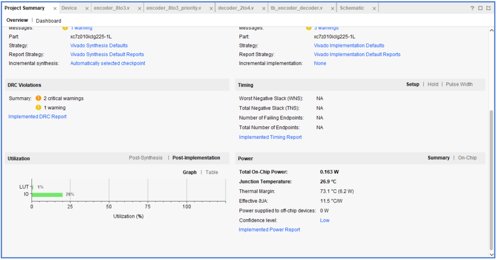
Step Ten: Synthesis
- Synthesizing the Design:
- In the “Flow Navigator” on the left side, under “Project Manager”, click on “Run Synthesis”.
- Vivado will process your design files to synthesize the circuit. This may take a few minutes.
- Upon completion, a dialog box will appear. Ensure to check “Run Implementation” and click “OK”.
[su_image_carousel source=”media: 899″ limit=”1″ captions=”yes” arrows=”no” dots=”no” link=”none” target=”blank” autoplay=”0″ image_size=”full” prefer_caption=”yes”]
[su_image_carousel source=”media: 900″ limit=”1″ captions=”yes” arrows=”no” dots=”no” link=”none” target=”blank” autoplay=”0″ image_size=”full” prefer_caption=”yes”]
Step Eleven: Implementation
- Running Implementation:
- The implementation process starts automatically after synthesis if you selected the option in the previous step.
- This step converts the synthesized design into a device-specific layout.
- Wait for the implementation to complete. This might take a while depending on the complexity of your design.
[su_image_carousel source=”media: 901″ limit=”1″ captions=”yes” arrows=”no” dots=”no” link=”none” target=”blank” autoplay=”0″ image_size=”full” prefer_caption=”yes”]
[su_image_carousel source=”media: 902″ limit=”1″ captions=”yes” arrows=”no” dots=”no” link=”none” target=”blank” autoplay=”0″ image_size=”full” prefer_caption=”yes”]
[su_image_carousel source=”media: 903″ limit=”1″ captions=”yes” arrows=”no” dots=”no” link=”none” target=”blank” autoplay=”0″ image_size=”full” prefer_caption=”yes”]
[su_image_carousel source=”media: 904″ limit=”1″ captions=”yes” arrows=”no” dots=”no” link=”none” target=”blank” autoplay=”0″ image_size=”full” prefer_caption=”yes”]
Step Twelve: Generating Bitstream (Optional, Required when Hardware is connected.)
- Generating the Bitstream:
- After implementation, in the “Flow Navigator”, click on “Generate Bitstream”.
- Vivado will now generate a bitstream file which is used to program the FPGA. Wait for this process to complete.
Step Thirteen: Opening Implemented Design
- Viewing the Implemented Design:
- Once the bitstream is successfully generated, go to “File” > “Open Implemented Design” to view the post-implementation layout of your design.
[su_image_carousel source=”media: 905″ limit=”1″ captions=”yes” arrows=”no” dots=”no” link=”none” target=”blank” autoplay=”0″ image_size=”full” prefer_caption=”yes”]
[su_image_carousel source=”media: 906″ limit=”1″ captions=”yes” arrows=”no” dots=”no” link=”none” target=”blank” autoplay=”0″ image_size=”full” prefer_caption=”yes”]
[su_image_carousel source=”media: 907″ limit=”1″ captions=”yes” arrows=”no” dots=”no” link=”none” target=”blank” autoplay=”0″ image_size=”full” prefer_caption=”yes”]
[su_image_carousel source=”media: 908″ limit=”1″ captions=”yes” arrows=”no” dots=”no” link=”none” target=”blank” autoplay=”0″ image_size=”full” prefer_caption=”yes”]
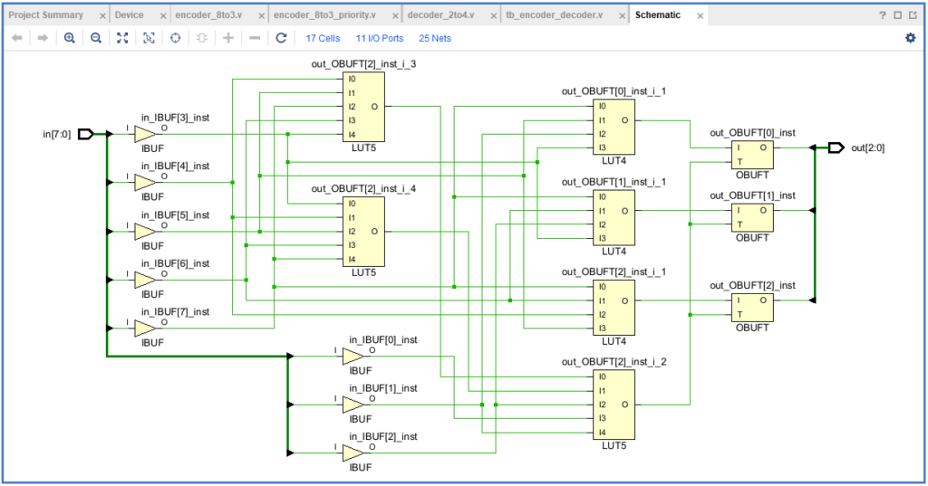
Step Fourteen: Checking Schematics
- Opening Schematic Viewer:
- With the implemented design open, in the “Flow Navigator”, under “Project Manager”, select “Schematic”. This opens the Schematic viewer.
- Use this tool to visually inspect the connections and components of your synthesized and implemented design. It helps in understanding the structure and for debugging purposes.
Step Fifteen: Launching Simulation Post-Implementation
- Simulating Post-Implementation Behavior (Optional):
- For a more thorough analysis, you can run a post-implementation simulation. Right-click on “Simulation” under “SIMULATION” in the “Flow Navigator” and select “Run Post-Implementation Simulation”.
- This simulation takes into account the actual device characteristics and timing information, providing a closer representation of real-world operation.
Step Sixteen: Analyzing and Saving Results
- Final Analysis:
- Review the simulation results, synthesized schematic, and implementation details to ensure your design meets the desired specifications and performance criteria.
- Make any necessary adjustments to your design based on this analysis.
Step Seventeen: Saving and Closing the Project
- Completion:
- Save your project and all changes by navigating to “File” > “Save Project”.
- Close Vivado by selecting “File” > “Close Project” or “File” > “Exit” when you’re finished with your session.
This procedure provides a hands-on approach to understanding the function and implementation of digital encoders and decoders within a simulated environment.
Additional Reading:
For those interested in diving deeper into CMOS VLSI design and digital logic simulations, resources like “Digital Design: With an Introduction to the Verilog HDL” by M. Morris Mano and Michael D. Ciletti provide a strong foundation.
FAQ:
- Q: Can I simulate other digital circuits in Vivado?
- A: Yes, Vivado supports a wide range of digital circuit simulations.
- Q: What is the importance of priority in encoders?
- A: Priority determines which input is considered when multiple inputs are active simultaneously.
Reference:
For more insights and resources related to this experiment, consider exploring the following:
- Internal Resource: Discover additional materials and experiments on VLSI design by visiting our JNTUH VLSI Lab page.
- External Resource: Access the complete source codes and further documentation for this lab session on our GitHub repository.
- Mano, M. M., & Ciletti, M. D. (2013). Digital Design: With an Introduction to the Verilog HDL. Pearson.